博文
半导体里程_博物馆_1974 量化集成电路工艺设计规则的缩放
|||
IBM公司的研究员罗伯特·迪纳德关于过程缩放型记忆的论文加速了收缩物理尺寸的全球竞赛和制造更复杂的集成电路。
在60年代,每个推进光刻能力面具尺寸的线性收缩提供一个快速解决提高速度和降低成本的集成电路。在1962年托马斯斯坦利的研究实验室发表的分析指出,由于其临界速度的极限尺寸,栅极长度,躺在横向而不是纵向平面双极器件,这是特别重要的金属氧化物半导体晶体管。
比例原则在布鲁斯卡弗·米德hoeneisen和加州理工学院的罗伯特迪纳德和他的同事的1972个文件被描述。由于登纳德等的1974个文件,引起微电子业界的关注与造成的深远影响。他们指出,由于晶体管的横向尺寸的比例系数,因相同的因素速度得到了提高。当时的绝缘性场效应管最小尺寸为5微米,他们预计缩小微米组分。(人的头发是50 - 100微米直径)这是第一次尝试将几何收缩所产生的结果降低功耗和性能改进。这给戈登穆尔(1965年)的“定律”提供了科学基础。
1976年,MITI组织公司,富士通日立,三菱、东芝,成一个联盟,超大规模集成电路技术研究协会,包括概念,缩放和结合日本光学和精细的制造优势在70年代末在全球范围内提供了64K动态随机存取存储器(1970的里程碑事件)。在这些高能晶体管上计算的功率消耗加快了互补金属氧化物半导体管技术的发展(1963的里程碑事件)。 这种尺寸互补金属氧化物半导体管的能力在2006年末允许尺寸收缩至100纳米(0.1微米)以下和像IBM公司/索尼/东芝的芯片为第三代游戏机提供了234000000个晶体管细胞处理器。

80年代中期IBM研究员
罗伯特·迪纳德 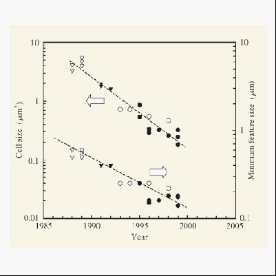
伴随最小特征尺寸内存单元尺寸的减小

100纳米cmos晶体管的扫描电镜图像

第三代游戏机23000000晶体管细胞处理器
译者:哈尔滨工业大学(威海)电子封装 090840224-宁尚佳
校对:哈尔滨工业大学(威海)电子封装 090840227-吴喆熹
原文
http://www.computerhistory.org/semiconductor/timeline/1974-Scaling.html
版权 copyright by www.computerhistory.org
————————————————————————————————
1974 - Scaling of IC Process Design Rules Quantified
IBM researcher Robert Dennard’s paper on process scaling on MOS memories accelerates a global race to shrink physical dimensions and manufacture ever more complex integrated circuits.
Linear shrinking of mask dimensions with each advance in lithographic capability provided a quick fix to enhance the speed and reduce the cost of ICs in the 1960s. Thomas Stanley of RCA Research Laboratories published an analysis in 1962 noting that this was particularly relevant to the MOS transistor because its critical speed limiting dimension, the length of the gate, lay in the horizontal rather than the vertical plane of bipolar devices.
Scaling principles were described in 1972 papers by Bruce Hoeneisen and Carver Mead of Caltech and by IBM's Robert Dennard and his colleagues. But it was a 1974 paper by Dennard, et. al. that caught the attention of the industry with a resulting profound effect on microelectronics. They noted that as the horizontal dimensions of a transistor were scaled by a factor, speed improved by that same factor. At a time when IBM's MOS memories used a minimum dimension of 5 microns, they projected shrinking to fractions of a micron. (A human hair is 50-100 microns in diameter) This was the first attempt to relate a geometry shrink to the resulting power reduction and performance improvement. It gave Gordon Moore's (1965 Milestone) "Law" a scientific foundation.
In 1976 MITI organized Hitachi, NEC, Fujitsu, Mitsubishi and Toshiba into a consortium, the VLSI Technology Research Association, that embraced the concept of scaling and combined it with Japanese optical and ultra-clean manufacturing strengths in a global race to deliver 64K DRAMs (1970 Milestone) by the end of the decade. Power consumption at these high transistor counts accelerated the adoption of CMOS technology. (1963 Milestone) The ability to scale CMOS allowed dimensions to shrink below 100 nanometers (0.1 micron) by 2006 and to deliver chips such as the IBM/Sony/Toshiba 234 million transistor Cell processor for the Playstation 3.
https://m.sciencenet.cn/blog-652849-544145.html
上一篇:半导体里程_博物馆_1978 用户可编程逻辑设备出现
下一篇:半导体里程_博物馆_1952 贝尔实验室授权晶体管技术