博文
半导体里程-博物馆-1954晶体管开发的扩散过程
|||
随着高温扩散的太阳能电池技术不断成熟,Charles Lee和Morris将该技术应用在了高速晶体管的制造中.
在1952年,贝尔实验室的化学家Calvin Fuller阐述了一种将杂质掺入硅和锗中的方法:通过与掺有所需杂质的高温气体接触使得硅和锗中掺入杂质。而且他通过调整曝光时间和温度,能精确地控制引入杂质的数量及其穿透深度,使其精度优于1微米,这种方法远远优于普通的P/N结生长技术。
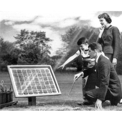
通过在1954年早期和工程师Daryl Chapin和物理学家Gerald Pearson在一起的工作,Fuller将扩散层的n型硅硼原子制作成晶片,在其表面下方形成了大面积的P/N结。通过对这些P/N结进行光照,他们产生了如OHL在1940年发现的那种来自光电效应的强电流,转换效率达到了6%。贝尔实验室于1954年4月26日发布了这种太阳能单元,并将其称为“太阳能电池”,这种太阳能单元被用于农村的电话系统以及空间卫星中。
在当年晚些时候查理斯•李利用扩散效应在仅仅几微米厚的基板上制作出了晶体管,这些晶体管的频率可被提升到170MHZ----是以往产品的十倍速度。在1955年3月,富勒采用向硅晶片中扩散进两种杂质的办法成功形成了N-P-N夹层,而化学家MORRIS TANENBAUM和他的研究生D.E.THOMAS制成了硅扩散晶体管。在1956年1月贝尔实验室专门针对上述技术和其他扩散技术开发了三极晶体管技术。


译者:哈尔滨工业大学(威海)电子封装 090840117-康志龙
校对:哈尔滨工业大学(威海)090840120-王开伟
原文:
1954 - Diffusion Process Developed for Transistors
Following the production of solar cells using high-temperature diffusion methods, Charles Lee and Morris Tanenbaum apply the technique to fabricate high-speed transistors.
Beginning in 1952 Bell Labs chemist Calvin Fuller demonstrated how impurities could be introduced into germanium and then silicon by exposing them to high-temperature gases containing desired dopants. By adjusting the time and temperature of exposure, he could precisely control the amount of impurities introduced and their penetration depth to accuracies of better than one micrometer — far better than achievable with grown-junction techniques.
Working with engineer Daryl Chapin and physicist Gerald Pearson in early 1954, Fuller diffused a layer of boron atoms into wafers of n-type silicon, forming large-area p-n junctions just beneath the surface. By shining light on these junctions, they generated a strong electric current via the photovoltaic effect discovered by Ohl in 1940, (1940 Milestone) getting energy conversion efficiencies up to 6 percent. Bell Labs announced this solar cell, dubbed the "Solar Battery," on 26 April 1954. By the late 1950s, solar cells were powering rural telephone systems and space satellites.
Later that year Charles Lee used diffusion to make transistors with base layers only a micrometer thick; they could operate at frequencies up to 170 MHz - ten times higher than earlier devices. And in March 1955, employing silicon wafers into which Fuller had diffused two different impurities to form a three-layer n-p-n sandwich, chemist Morris Tanenbaum and his technician D. E. Thomas fabricated silicon diffused-base transistors. In January 1956 Bell Labs held a third symposium on transistor technology (1952 Milestone) specifically devoted to these and other diffusion techniques.
copyright by www.computerhistory.org
https://m.sciencenet.cn/blog-652849-544761.html
上一篇:半导体里程_博物馆_1953晶体管计算机的出现
下一篇:半导体里程_博物馆_1954_硅晶体管提供优越的工作特性