博文
半导体里程_博物馆_ 1967-专用集成电路采用电脑辅助设计
|||
用自动化设计工具减少开发工程的时间和设计,并提供复杂的定制集成电路
随着英特网共享连接变得复杂化,他们的设计和生产周期延伸到好几年,而一些最终产品寿命周期缩短到一个季度。1967年,为了加快美国空军大批量复合定制电路的生产速度,IBM和德州仪器开发了“自行分配布线”的方法,采用唯一的一台计算机生成(1966年里程碑)每个晶圆金属掩模的技术。 为量产定制设计开发的两种方法是门阵列和标准单元 。他们统称为特定应用集成电路(ASIC)。门阵列是无连接的晶体管的晶片片生产技术。最终定制互连技术确定为最后的生产方案,虽然它比手工制作芯片的硅使用效率低,但是雏形可以从几个月的生产周期缩短为几天。早期门阵列供应商,如费伦蒂/协调会是手工的定制连接。1967年,飞兆半导体公司在推出微矩阵系列——双极DTL和TTL电阵列,此阵列可用CAD工具来执行两者的相互操作。1974年, 罗伯特·利普为国际集成电路设计了第一款CMOS阵列,但是可行的CAD支持在若干年后也没人设计出来。标准单元的英特尔网络共享连接采用了一系列应用了装配目录功能设计的制造板罩,并存储在电脑存储信息库中。他们提供了一个硅高效的手工设计和门阵列的快速掉头之间的折中的方法。飞兆半导体和摩托罗拉提供的一个早期的MOS标准单元权限低于商品牌号Miscromosaic和Polycell。超大规模集成电路技术(成立于1979年)和LSI Logic(1981)成功地利用20世纪70年代被遗弃的CAD为基础的ASIC概念。当时被摒弃就是因为花费大量的计算时间。
Fairchild 4500 - a 1967 DTL 32-gate Micromatrix custom array designed using CAD tools to interconnect two layers of metal
飞兆半导体4500 - 1967年DTL32门的Micromatrix自定义数组使用CAD工具设计,两层金属互连
Credit: Fairchild Camera & Instrument Corporation
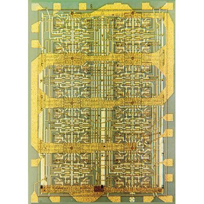
Micromosaic - a 1968 standard cell design for GE Avionics. One of the industry's first designs for revenue
micromosaic - 1968年为GE航空电子标准电池的设计。一个行业的第一个设计收入
Credit: Fairchild Camera & Instrument Corporation

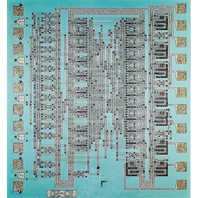
IBM LSI MOD1, an experimental discretionary-wired wafer design by IBM fabricated by Texas Instuments
IBM LSI MOD1,由IBM酌情-连接的实验晶片设计由德州自控制作
Credit: International Business Machines Corporation

A Ferranti ULA (Uncommitted Logic Array) integrated 14 TTL IC packages for the Sinclair ZX81 PC in 1981
一个费伦蒂ULA(自由逻辑阵列)集成了14组TTL IC封装在1981年辛克莱ZX81 PC
Credit: Sinclair Research
1967 - Application Specific Integrated Circuits employ Computer-Aided Design
Automated design tools reduce the development engineering time to design and deliver complex custom integrated circuits.
As ICs increased in complexity their design and manufacturing turn-around times stretched out to years even as some end product life cycles shrank to a single season. To speed the availability of prototype quantities of complex custom circuits for the Air Force in 1967 IBM and Texas Instruments developed “discretionary-wiring” approaches that employed a unique computer-generated (1966 Milestone) metal mask for every wafer.Two approaches developed for volume production of custom designs are gate arrays and standard cells - collectively known as Application-Specific ICs (ASIC). Gate arrays are produced as wafers of unconnected transistors. As the customizing interconnections are applied at the final manufacturing step, although less efficient in silicon usage than handcrafted chips, prototypes can be produced in days rather than months. Early gate array suppliers such as Ferranti/Interdesign designed the custom connections manually. In 1967 Fairchild introduced the Micromatrix family of bipolar DTL and TTL arrays that used CAD tools to perform this operation interactively. Robert Lipp designed the first CMOS array for International Microcircuits in 1974 but viable CAD support was not forthcoming for several years. Standard cell ICs employ a full set of fabrication masks using designs assembled from catalog functions stored in a computer library.They offer a compromise between silicon-efficient handcrafted designs and the fast turn-around of gate arrays.Fairchild and Motorola offered early MOS standard cell capabilities under the trade names Micromosaic and Polycell. VLSI Technology (founded 1979) and LSI Logic (1981) successfully exploited these CAD-based ASIC concepts abandoned by the original vendors in early 1970s largely due to the then high cost of computing time.
译者:哈尔滨工业大学(威海)电子封装 090840215申聪敏
校对:哈尔滨工业大学(威海)电子封装 090840214 葛峰
原文:http://www.computerhistory.org/semiconductor/timeline/1967-ASICs.html
版权:copyright by www.computerhistory.org
https://m.sciencenet.cn/blog-652849-545403.html
上一篇:半导体里程_博物馆_36集成电路
下一篇:半导体-博物馆-1967-核心设备供应商改变工业动向