博文
半导体里程_博物馆_1951_ 第一生长结晶体管的制备
|||
在威廉·肖克利的PN结理论被验证之后(1948年),制造一个可以工作的结型晶体管仍然面临严峻的挑战。主要问题是缺乏足够纯净,均匀的半导体材料。贝尔实验室的化学家戈登·蒂尔认为,将需要大的单晶,锗和硅,但听从的人很少,包括肖克利。
在管理层很少的支持下,蒂尔建立自己所需的晶体生长设备,在机械工程师约翰小和欧内斯特·比埃勒技术员的帮助下。 他在1917年由波兰化学家Jan Czochralski开发的技术的基础上,用一个小的“种子”锗晶体在坩埚熔锗中慢慢地缩回来,形成一个狭长的单晶。 肖克利这一成就后来被称为 “在初期半导体领域最重要的科学成果。
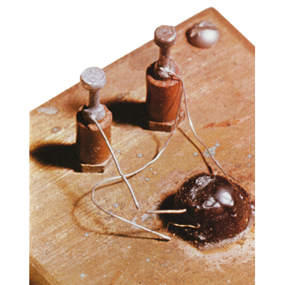
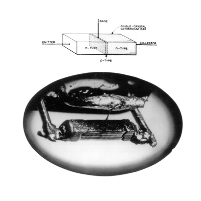
采用这种技术,贝尔实验室的化学家Morgan Sparks通过在熔融锗晶体生长过程中加入微小颗粒杂质,制作pn结。 在1950年4月,他和蒂尔开始向熔体中加入两个连续的小球,第一个是p型杂质和第二个是n型杂质,形成了内层很薄的NPN结构。 一年后,这种“生长出的结型晶体管”超越性能最好的点接触晶体管。在1951年7月4日, 贝尔实验室在一次会议上宣布了这一发现,并强调了肖克利的贡献。
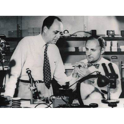
Gordon K. Teal(左)和Morgan Sparks在贝尔实验室,1951年
2006-2007 Alcatel-Lucent. All rights reserve
Courtesy of: Jack Ward - Transistor Museum
译者:哈尔滨工业大学(威海)电子封装 090840111-计孝智
校对:哈尔滨工业大学(威海)电子封装 090840114-刘继伟
版权 copyright by www.nobeprize.org
原文:http://www.computerhistory.org/semiconductor/timeline/1951-First.html
After William Shockley’s theories about p-n junctions had been validated by tests (1948 Milestone), fabricating a working junction transistor still presented formidable challenges. The main problem was lack of sufficiently pure, uniform semiconductor materials. Bell Labs chemist Gordon Teal argued that large, single crystals of germanium and silicon would be required, but few - including Shockley - were listening.
With little support from management, Teal built the needed crystal-growing equipment himself, with help from mechanical engineer John Little and technician Ernest Buehler. Based on techniques developed in 1917 by the Polish chemist Jan Czochralski, he suspended a small "seed" crystal of germanium in a crucible of molten germanium and slowly withdrew it, forming a long, narrow, single crystal. Shockley later called this achievement "the most important scientific development in the semiconductor field in the early days."
Employing this technique, Bell Labs chemist Morgan Sparks fabricated p-n junctions by dropping tiny pellets of impurities into the molten germanium during the crystal-growing process. In April 1950, he and Teal began adding two successive pellets into the melt, the first with a p-type impurity and the second n-type, forming n-p-n structures with a thin inner, or base, layer. A year later, such “grown-junction transistors” surpassed the best point-contact transistors in performance. Bell Labs announced this advance on July 4, 1951 in a press conference featuring Shockley.
https://m.sciencenet.cn/blog-652849-546086.html
上一篇:半导体里程_博物馆_1971 – 将微处理器的功能集成到一个CPU芯片
下一篇:半导体里程_博物馆_开关
全部精选博文导读
相关博文
- • Minerals线下恳谈会:履践致远、与时偕行——对话中国科学院广州地球化学研究所期刊合作学者
- • 聚英才 建高地 | 北京理工大学“特立青年学者”全球招聘开启
- • 700年后日本或濒临灭绝?日本学者推算预测:届时或仅剩1名15岁以下孩子
- • [转载]【同位素视角】非英语母语学者如何区分’e.g.’, ‘i.e.’, ‘namely’与‘such as’等混淆难题
- • 美国佐治亚大学等机构学者:刈割策略对Bulldog 805紫花苜蓿+Tifton 85狗牙根混播草地产量及品质的影响
- • 美国堪萨斯州立大学、密苏里大学等机构学者研究成果:土壤水分管理策略和品种多样性对紫花苜蓿产量、营养品质和农场盈利能力的影