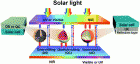
研究人员测量了低成本半导体近乎完美的性能 诸平 据 斯坦福大学 (Stanford University) 2019年3月15日提供的信息,该大学的研究人员开发出一种测量技术,测量了低成本半导体近乎完美的性能。 在太阳能电池板、相机传感器和医学成像工具中发现的先进电子产品中,被称为量子点的微小、易于生产的粒子,很可能很快就会取代更昂贵的单晶半导体。尽管量子点已经开始以量子点电视的形式进入消费市场,但长期以来,量子点电视的质量一直存在不确定性,阻碍了其发展。现在,斯坦福大学的研究人员开发的一种新的测量技术可能最终会消除这些疑虑。 斯坦福大学化学研究生戴维·哈尼菲(David Hanifi)说:“传统半导体是单晶,在真空中特殊条件下生长。我们可以在实验室里的烧瓶中大量制造量子点,我们已经证明它们和最好的单晶一样好。” 研究人员专注于量子点如何有效地重新发射它们所吸收的光,这是衡量半导体质量的一个指标。虽然之前对量子点效率的研究暗示了量子点的高性能,但这是第一个自信地证明量子点可以与单晶竞争的测量方法。这项研究是美国斯坦福大学 (Stanford University) 、劳伦斯·伯克利国家实验室(Lawrence Berkeley National Laboratory)、加州大学伯克利分校(University of California, Berkeley), 日本有关公司(High Performance Materials Company, JXTG Nippon Oil Energy Corporation)、比利时哈瑟尔特大学(Hasselt University)、荷兰埃因霍温理工大学(Eindhoven University of Technology)以及美国的卡佛利能源纳米科学研究所(Kavli Energy NanoScience Institute)合作完成的,相关研究结果,2019年3月15日已经在《科学》(Science)杂志网站发表——David A. Hanifi, Noah D. Bronstein, Brent A. Koscher, Zach Nett, Joseph K. Swabeck, Kaori Takano, Adam M. Schwartzberg, Lorenzo Maserati, Koen Vandewal, Yoeri van de Burgt, Alberto Salleo, A. Paul Alivisatos. Redefining near-unity luminescence in quantum dots with photothermal threshold quantum yield. Science , 15 Mar 2019: Vol. 363, Issue 6432, pp. 1199-1202. DOI: 10.1126/science.aat3803 加州大学伯克利分校的纳米科学和纳米技术的三星特聘教授,量子点的先驱研究者 Paul Alivisatos,也是论文的通讯作者,他强调了此测量技术如何能够引领新技术和新材料的发展,而这些新技术和新材料要求我们在很大程度上了解半导体的效率。 “这些材料的效率如此之高,以至于现有的测量无法量化它们到底有多好。这是一个巨大的飞跃。“也许有一天,它可以应用于需要发光效率远高于99%的材料的应用,而这些材料中的大多数还没有被发明出来。”更多信息敬请注意浏览原文或者相关报道 Between 99 and 100 Being able to forego the need for pricey fabrication equipment isn't the only advantage of quantum dots. Even prior to this work, there were signs that quantum dots could approach or surpass the performance of some of the best crystals. They are also highly customizable. Changing their size changes the wavelength of light they emit, a useful feature for color-based applications such as tagging biological samples, TVs or computer monitors. Despite these positive qualities, the small size of quantum dots means that it may take billions of them to do the work of one large, perfect single crystal. Making so many of these quantum dots means more chances for something to grow incorrectly, more chances for a defect that can hamper performance. Techniques that measure the quality of other semiconductors previously suggested quantum dots emit over 99 percent of the light they absorb but that was not enough to answer questions about their potential for defects. To do this, the researchers needed a measurement technique better suited to precisely evaluating these particles. We want to measure emission efficiencies in the realm of 99.9 to 99.999 percent because, if semiconductors are able to reemit as light every photon they absorb, you can do really fun science and make devices that haven't existed before, said Hanifi. The researchers' technique involved checking for excess heat produced by energized quantum dots, rather than only assessing light emission because excess heat is a signature of inefficient emission. This technique, commonly used for other materials, had never been applied to measure quantum dots in this way and it was 100 times more precise than what others have used in the past. They found that groups of quantum dots reliably emitted about 99.6 percent of the light they absorbed (with a potential error of 0.2 percent in either direction), which is comparable to the best single-crystal emissions. It was surprising that a film with many potential defects is as good as the most perfect semiconductor you can make, said Salleo, who is co-author of the paper. Contrary to concerns, the results suggest that the quantum dots are strikingly defect-tolerant. The measurement technique is also the first to firmly resolve how different quantum dot structures compare to each other—quantum dots with precisely eight atomic layers of a special coating material emitted light the fastest, an indicator of superior quality. The shape of those dots should guide the design for new light-emitting materials, said Alivisatos. Entirely new technologies This research is part of a collection of projects within a Department of Energy-funded Energy Frontier Research Center, called Photonics at Thermodynamic Limits. Led by Jennifer Dionne, associate professor of materials science and engineering at Stanford, the center's goal is to create optical materials—materials that affect the flow of light—with the highest possible efficiencies. A next step in this project is developing even more precise measurements. If the researchers can determine that these materials reach efficiencies at or above 99.999 percent, that opens up the possibility for technologies we've never seen before. These could include new glowing dyes to enhance our ability to look at biology at the atomic scale, luminescent cooling and luminescent solar concentrators, which allow a relatively small set of solar cells to take in energy from a large area of solar radiation. All this being said, the measurements they've already established are a milestone of their own, likely to encourage a more immediate boost in quantum dot research and applications. People working on these quantum dot materials have thought for more than a decade that dots could be as efficient as single crystal materials , said Hanifi, and now we finally have proof. Superefficient light emission A challenge to improving synthesis methods for superefficient light-emitting semiconductor nanoparticles is that current analytical methods cannot measure efficiencies above 99%. Hanifi et al. used photothermal deflection spectroscopy to measure very small nonradiative decay components in quantum dot photoluminescence. The method allowed them to tune the synthesis of CdSe/CdS quantum dots so that the external luminescent efficiencies exceeded 99.5%. This is important for applications that require an absolute minimum amount of photon energy to be lost as heat, such as photovoltaic luminescent concentrators. Science , this issue p. 1199 Abstract A variety of optical applications rely on the absorption and reemission of light. The quantum yield of this process often plays an essential role. When the quantum yield deviates from unity by significantly less than 1%, applications such as luminescent concentrators and optical refrigerators become possible. To evaluate such high performance, we develop a measurement technique for luminescence efficiency with sufficient accuracy below one part per thousand. Photothermal threshold quantum yield is based on the quantization of light to minimize overall measurement uncertainty. This technique is used to guide a procedure capable of making ensembles of near-unity emitting cadmium selenide/cadmium sulfide (CdSe/CdS) core-shell quantum dots. We obtain a photothermal threshold quantum yield luminescence efficiency of 99.6 ± 0.2%, indicating nearly complete suppression of nonradiative decay channels.
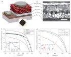
单层 MoS 2 量子点的新颖合成方法 钟伟 2017-10-18 MoS 2 纳米片作为一种重要的类石墨烯半导体二维材料,优异的物理、化学性质使其在众多领域具有广泛的潜在应用,因此引起人们极大的研究兴趣。在众多的制备方法中,超声液相剥离法操作简单,制备条件要求不高,而且剥离后能很好的保持材料原本的晶体结构,是最有希望实现大规模工业生产的一种制备方法。 超声液相剥离法是以 MoS 2 粉体为原料,在合适的溶剂中,通过调节超声参数产生较强的空化效应,对块体 MoS 2 进行剥离和分散从而获得 MoS 2 纳米片的方法。我们采用 南京先欧科技公司( ATPIO ) 生产的超声微波协同反应工作站( XO-SM50 ), 研究了不同的超声功率对块体 MoS 2 剥离程度及纳米片质量的影响(图1)。 Fig. 1Dispersions of MoS2 prepared with different ultrasonic power intensities. (a)UV-vis absorption spectra of MoS2 dispersions in NMP prepared with 100, 200,250, 285, 320, 350 and 400 W, respectively. In all the cases, the spectra areshown as measured absorbance, A, divided by cell length, l. Inset in (a) showsthe same spectra on a log–log scale. A straight dash line in the highwavelength region of this plot indicates a scattering background. (b) A/lsubtracted background for each sample of A excitonic peak is plotted as afunction of ultrasonic power. (c) Scattering exponent, n, as a function ofultrasonic power. Inset in (c) shows the variation of the position of Aexcitonic peaks (lA). (d) Image of the final dispersions after allowing them tostand for several weeks. 研究结果表明,随着超声功率的增加,悬浮液的浓度先增加,在 320 W 功率下浓度最高,超过 320 W ,浓度显著地下降。从 100 W 至 250 W ,纳米片的尺寸减小, 200 W 和 250 W 情况下,尺寸大多小于 60 nm ,且尺寸分布较均匀, 285 W 以后略有增加; 350 W 后,纳米片的平均横向尺寸的急剧增加。这种变化是由于空化泡引起的微射流敲击强度受到大量气泡散射的结果(图2)。 Fig. 2(a) Illustration of the two types of cavitation mechanism. (b) Mean flakelength and width (based on more than 300 randomly selected nanoflakes for eachsample) obtained at different ultrasonic power intensities. (c) Schematicrepresentation of the exfoliation procedure to obtain MoS2 nanoflakes in fourdistinct regions (I to IV). (d) Images of the acoustic cavitation bubbles inNMP solvent at different input powers. (e) SEM images of the sediment aftercentrifugation of 100, 200, 285 and 400 W samples. 为了获得单层量子点,我们采用 Li 离子插层法剥离 MoS 2 ,具体制备步骤如下: 1 、取 MoS 2 原粉放入圆底三口烧瓶中,滴入正己烷,烧瓶内通氩气保护。快速取丁基锂正己烷溶液放入圆底烧瓶内,将混合的 MoS 2 原粉和丁基锂正己烷溶液静置 2 天,使锂充分插入 MoS 2 层间,形成插层化合物 LixMoS 2 。 2 、真空抽滤插层的 LixMoS 2 ,并用正己烷多次清洗去除多余的丁基锂及有机残余物。 3 、快速取出抽滤膜上的 LixMoS 2 ,使之与去离子水反应,液体中会有大量气泡产生,为 LixMoS 2 与水反应生成的氢气。与水反应后,放入 超声微波协同反应工作站 ( XO-SM50 )中在 180 W 的功率下辅助超声 1 h ,即可获得单层的 MoS 2 纳米片悬浮液。 图 3 单次 Li 离子插层剥离过程示意图 我们发现,初始的 MoS 2 粉体尺寸在几微米至几十微米量级,经过一次插层剥离以后,得到的纳米片的尺寸在 100-800 nm 之间,尺寸明显减小,因此,如果将一次剥离的纳米片干燥重堆积后进行再次剥离,重复几次,最终即可以得到纳米级量子点。 干燥后重堆积的 MoS 2 纳米片重复上面的步骤进行第二次、第三次 Li 离子插层剥离,如图 4 所示。最终得到平均粒径 3 nm ,粒径分布窄且为单层的 MoS 2 量子点。 Fig. 4.Schematic illustration of the preparation of monolayer MoS 2 QDs using multipleexfoliation with Li intercalation. 相关研究工作成果,详见以下论文: 1. “Effects of ultrasonic cavitationintensity on the efficient liquid-exfoliation of MoS2 nanosheets” W. Qiao, S.M.Yan, X.M. He, X.Y. Song, Z.W. Li, X. Zhang, W. Zhong *, You-Wei Du, RSC Advances 4 (92), 50981-50987(2014) 2. “Enhancement of magnetism bystructural phase transition in MoS2”, S. M. Yan, W. Qiao, X.M. He, X.B. Guo, L.Xi, W. Zhong* , Y. W. Du, Appl. Phys. Lett. , 106 (1) , 012408(2015) 3. “Luminescent monolayer MoS2quantumdots produced by multi-exfoliation based on lithium intercalation”, W. Qiao,S.M. Yan, X.Y. Song, X. Zhang, X.M. He, W.Zhong *, Y.W. Du, Applied Surface Science 395, 130-136(2015) 4. “Monolayer MoS2 quantum dots ascatalysts for efficient hydrogen evolution”, W. Qiao, S.M. Yan, X.Y. Song, X.Zhang, Y. Sun, X. Chen, W. Zhong *,Y.W. Du, RSC Advances 5, 97696-97701 (2015)
Fluorescent Nanomaterial-derived White Light-Emitting Diodes: What’s Going On Qiang Zhang , Cai-Feng Wang , Lu-Ting Ling and Su Chen * First published online 25 Mar 2014, J. Mater. Chem. C , 2014, 2(22): 4358-4373 链接: http://pubs.rsc.org/en/content/articlelanding/2014/tc/c4tc00048j#!divAbstract 白光LED以长寿命、节能效果显著的优越性能,成为可替代传统白炽灯的新一代照明产品,因此近年来受到广泛关注。文章主要总结了近几年 Prof. Chen 课题组及国际上其他课题组在该领域的一些进展。在前人的基础上,扩充了光转换材料的范围。涉及到的白光LED转换材料主要包括半导体量子点、硅量子点、碳量子点、石墨烯量子点、荧光纳米有机无机和材料(量子点-聚合物、荧光薄膜)等,对此方向上的主要研究进展进行了客观的总结和评述。 1. 量子点 1.1 半导体量子点 1.2 核/多壳结构 1.3 掺杂量子点 1.4 无重金属量子点 1.5 直接白光发射的量子点 2. 碳量子点 3.1 电致发光碳量子点LED 3.2 光致发光碳量子点LED 3.3 白光碳量子点基LED 3. 硅量子点 4. 石墨烯量子点 5. 有机无机杂化白光LED 5.1 量子点-共轭聚合物杂化电致发光WLED 5.2 量子点-聚合物杂化光致发光WLED 5.3 半导体量子点-聚合物荧光薄膜(远程) 5.4 碳量子点-聚合物荧光薄膜(远程) Timeline showing recent progress in fluorescent nanomaterial-derived white LEDs. Abstract: White light-emitting diodes (white LEDs) have recently attracted substantial interest owing to their remarkable energy conservation. The evolution of fluorescent nanomaterials with tunable optical properties has provided an opportunity for light source design of white LEDs. However, the stability and performance of fluorescent nanomaterial-derived white LEDs still fail to meet the requirements of practical applications. It is therefore imperative to boost their overall device performance, which depends on not only the exploitation of advanced fluorescent nanomaterials but also the design of superior light source. In this review, the achievements in fluorescent nanomaterials as color converters towards white LEDs are highlighted, including semiconductor nanocrystals or colloidal quantum dots (QDs), carbon-based nanoparticles, silicon QDs, and organic-inorganic fluorescent nanocomposites. The challenges and future perspectives in this research area are also discussed.
最近,我们在 Chemical Society Reviews 上发表了题为Enhancing solar cell efficiency: the search for luminescent materials as spectral converters 的综述。 http://pubs.rsc.org/en/content/articlelanding/2013/CS/C2CS35288E Photovoltaic (PV) technologies for solar energy conversion represent promising routes to green and renewable energy generation. Despite relevant PV technologies being available for more than half a century, the production of solar energy remains costly, largely owing to low power conversion efficiencies of solar cells. The main difficulty in improving the efficiency of PV energy conversion lies in the spectral mismatch between the energy distribution of photons in the incident solar spectrum and the bandgap of a semiconductor material. In recent years, luminescent materials, which are capable of converting a broad spectrum of light into photons of a particular wavelength, have been synthesized and used to minimize the losses in the solar-cell-based energy conversion process. In this review, we will survey recent progress in the development of spectral converters, with a particular emphasis on lanthanide-based upconversion, quantum-cutting and down-shifting materials, for PV applications. In addition, we will also present technical challenges that arise in developing cost-effective high-performance solar cells based on these luminescent materials. TOC
Quantum Dot Capped Magnetite Nanorings as High Performance Nanoprobe for Multiphoton Fluorescence and Magnetic Resonance Imaging Authors: Hai-Ming Fan,* Malini Olivo, Borys Shuter, Jia-Bao Yi, Ramaswamy Bhuvaneswari, Hui-Ru Tan, Gui-Chuan Xing, Cheng-Teng Ng, Lei Liu, Sasidharan S. Lucky, Boon-Huat Bay, and Jun Ding 期刊 : J. Am. Chem. Soc . 2010, 132, 1480314811 摘要: In the present study, quantum dot (QD) capped magnetite nanorings (NRs) with a high luminescence and magnetic vortex core have been successfully developed as a new class of magneticfluorescent nanoprobe. Through electrostatic interaction, cationic polyethylenimine (PEI) capped QD have been firmly grafted into negatively charged magnetite NRs modified with citric acid on the surface. The obtained biocompatible multicolor QD capped magnetite NRs exhibit a much stronger magnetic resonance (MR) T2* effect where the r2* relaxivity and r2*/r1 ratio are 4 times and 110 times respectively larger than those of a commercial superparamagnetic iron oxide. The multiphoton fluorescence imaging and cell uptake of QD capped magnetite NRs are also demonstrated using MGH bladder cancer cells. In particular, these QD capped magnetite NRs can escape from endosomes and be released into the cytoplasm. The obtained results from these exploratory experiments suggest that the cell-penetrating QD capped magnetite NRs could be an excellent dual-modality nanoprobe for intracellular imaging and therapeutic applications. This work has shown great potential of the magnetic vortex core based multifunctional nanoparticle as a high performance nanoprobe for biomedical applications. 简评: 氧化铁纳米环的合成和制备已经在前期报道了很多。其特殊的形貌结构导致了稳定涡旋磁态(vortex state)的存在,这个vortex state 在外场的作用下可以磁化转成onion state。涡旋磁态的存在和 两个态之间的transition在过去5年已经在包括Science, PRL 等一系列顶级杂志中发表的论文里进行了详细的讨论。 然后其应用领域尚未有所突破,近期在nature physics上有论文报道关于利用vortex spin有效杀死癌症细胞的例子。本文利用其涡旋磁态时,颗粒之间弱的磁相互作用形成了较稳定的水相分散体,并嫁接了荧光量子点赋予其光学性能。这个复合的纳米环定义为,QD-FVIOs. 其中FVIO is ferrimagnetic/ferromagnetic vortex-state iron oxides.在磁共振成像的表征上发现,相对于超顺磁的氧化铁,涡旋磁态氧化铁表现了非常高的T2*效应。细胞荧光成像实验和MRI成像实验结果表明,这种基于vortex state 的纳米磁环结构在生物医学和细胞成像(cell imaging)上有着很大的用途。详情请参考论文。
In this paper, based on selecting the appropriate type of quantum dots (QDs), a novel method is developed to enhance the quantum yield (QY) of silica-coated QD nanoparticles (SQDNPs). The effect of varying types of QDs on the QY after silica encapsulation is systematically studied. The results show that QDs with appropriate structure and composition of shells can much better retain the initial QY after silanization. The seven-layered shell/core QDs with QY of 47.8% nearly completely retain the original QY and is the best type among six types of QDs for silica modification. In the aspect of shell composition, the CdS plays an important role for QY retention since the lattice mismatch between CdSe and CdS is lower than that of CdSe and ZnS. After the appropriate type of QDs is chosen for silica coating, the highly fluorescent SQDNPs are chemically modified with amine, thiol and carboxyl groups, and then labeled by antibodies for particle-based immunofluorescence assay. The results indicate that the SQDNPsantibody bioconjugates are alternative fluorescent probes useful for biodetection. http://www.iop.org/EJ/abstract/0957-4484/19/46/465604
 标签: 量子点