Special Collection:石墨烯和其他二维材 料 近十年来,自 K. Novoselov 和 A. Geim 发现石墨烯以来,由于其引人注目的特性,致力于石墨烯和其他二维材料的研究工作如火如荼。 K. Novoselov 和 A. Geim 亦因 “ 二维材料石墨烯的开创性实验 ” 摘取 2010 年诺贝尔物理学奖。近年来对石墨烯的研究进一步激发了研究人员对于其他二维材料的极大兴趣。在石墨烯之外的这些新材料中,其直系表亲硅烯和锗(硅和锗的对应物)得到了特别关注。 这些材料的低能量理论可以由類石墨烯的狄拉克费米子哈密尔顿量所描述,因此其相对较强的自旋 - 轨道相互作用大到足以使诸如硅基和锗基的材料成为非平凡的拓扑绝缘体。 此外,对单层过渡金属二硫属元素化物和层状双过渡金属碳 / 氮化物( MXenes )的研究也越来越受到关注。 由诺贝尔物理学奖得主、英国曼彻斯特大学 Kostya Novoselov 教授领衔,与新加坡国立大学 Daria Andreeva 教授、中科院金属所任文才教授和北航单光存教授合作为 FOP 刊组织了专题 “Graphene and other Two-Dimensional Materials” 。这一专题涵盖 2D 材料的实验合成、实验表征( ARPES , STM ,光学吸收等)、电学特性、电磁微波吸收特性、光学特性、磁学特性、拓扑特性及潜在应用等方面。文章已陆续上线,将分两部分刊载。 Special Collection: Graphene and other Two-Dimensional Materials (Part I) (Eds. Daria Andreeva, Wencai Ren, Guangcun Shan Kostya Novoselov) REVIEW The rise of two-dimensional MoS 2 for catalysis Jun Mao ( 毛军 ), Yong Wang ( 王勇 ), Zhilong Zheng ( 郑智龙 ), and Dehui Deng ( 邓德会 )* Abstract: Two-dimensional (2D) MoS 2 is used as a catalyst or support and has received increased research interest because of its superior structural and electronic properties compared with those of bulk structures. In this article, we illustrate the active sites of 2D MoS 2 and various strategies for enhancing its intrinsic catalytic activity. The recent advances in the use of 2D MoS 2 –based materials for applications such as conventional heterogeneous catalysis, electrocatalysis, and photocatalysis are discussed. We also discuss the future opportunities and challenges for 2D MoS 2 –based materials, in both fundamental research and industrial applications. REVIEW Environmental engineering of transition metal dichalcogenide optoelectronics Trevor LaMountain, Erik J. Lenferink, Yen-Jung Chen, Teodor K. Stanev, and Nathaniel P. Stern* Abstract: The explosion of interest in two-dimensional van der Waals materials has been in many ways driven by their layered geometry. This feature makes possible numerous avenues for assembling and manipulating the optical and electronic properties of these materials. In the specific case of the monolayer transition metal dichalcogenide semiconductors, the direct band gap combined with the exibility for manipulation of layers has made this class of materials promising for optoelectronics. Here, we review the properties of these layered materials and the various means of engineering their properties for optoelectronics. We summarize approaches to control using their structural and chemical environment, and we give particular detail on the integration of these materials into engineered optical fields to control their optical characteristics. This combination of controllability from their layered surface structure and photonic environment provide an expansive landscape for novel optoelectronic phenomena. REVIEW Two-dimensional materials: Emerging toolkit for construction of ultrathin high-efficiency microwave shield and absorber Mingjun Hu * , Naibai Zhang, Guangcun Shan, Jiefeng Gao, Jinzhang Liu, and Robert K. Y. Li* Abstract: Two-dimensional (2D) materials generally have unusual physical and chemical properties owing to the confined electro-strong interaction in a plane and can exhibit obvious anisotropy and a significant quantum-confinement effect, thus showing great promise in many fields. Some 2D materials, such as graphene and MXenes, have recently exhibited extraordinary electromagnetic-wave shielding and absorbing performance, which is attributed to their special electrical behavior, large specific surface area, and low mass density. Compared with traditional microwave attenuating materials, 2D materials have several obvious inherent advantages. First, similar to other nanomaterials, 2D materials have a very large specific surface area and can provide numerous interfaces for the enhanced interfacial polarization as well as the reflection and scattering of electromagnetic waves. Second, 2D materials have a particular 2D morphology with ultrasmall thickness, which is not only beneficial for the penetration and dissipation of electromagnetic waves through the 2D nanosheets, giving rise to multiple reflections and the dissipation of electromagnetic energy, but is also conducive to the design and fabrication of various well-defined structures, such as layer-by-layer assemblies, core–shell particles, and porous foam, for broadband attenuation of electromagnetic waves. Third, owing to their good processability, 2D materials can be integrated into various multifunctional composites for multimode attenuation of electromagnetic energy. In addition to behaving as microwave reflectors and absorbers, 2D materials can act as impedance regulators and provide structural support for good impedance matching and setup of the optimal structure. Numerous studies indicate that 2D materials are among the most promising microwave attenuation materials. In view of the rapid development and enormous advancement of 2D materials in shielding and absorbing electromagnetic wave, there is a strong need to summarize the recent research results in this field for presenting a comprehensive view and providing helpful suggestions for future development. RESEARCH Monolayered semiconducting GeAsSe and SnSbTe with ultrahigh hole mobility Yu Guo, Nan Gao, Yizhen Bai, Jijun Zhao * , and Xiao Cheng Zeng* (Cover story) Abstract: High carrier mobility and a direct semiconducting band gap are two key properties of materials for electronic device applications. Using first-principles calculations, we predict two types of two-dimensional semiconductors, ultrathin GeAsSe and SnSbTe nanosheets, with desirable electronic and optical properties. Both the GeAsSe and SnSbTe sheets are energetically favorable, with formation energies of −0.19 and −0.09 eV/atom, respectively, and have excellent dynamical and thermal stability, as determined by phonon dispersion calculations and Born–Oppenheimer molecular dynamics simulations. The relatively weak interlayer binding energies suggest that these monolayer sheets can be easily exfoliated from the bulk crystals. Importantly, monolayer GeAsSe and SnSbTe possess direct band gaps (2.56 and 1.96 eV, respectively) and superior hole mobility ( ~ 20 000 cm 2 × V −1 × s −1 ), and both exhibit notable absorption in the visible region. A comparison of the band edge positions with the redox potentials of water reveals that layered GeAsSe and SnSbTe are potential photocatalysts for water splitting. These exceptional properties make layered GeAsSe and SnSbTe promising candidates for use in future high-speed electronic and optoelectronic devices. RESEARCH Interfacial charge transfer in WS 2 monolayer/CsPbBr 3 microplate heterostructure Zhen-Zhong Yan, Zhao-Han Jiang, Jun-Peng Lu * , and Zhen-Hua Ni Abstract: Integration of heterogenous materials produces compelling physical phenomena and increased performance of optoelectronic devices. In this work, we integrate CsPbBr 3 microplate with WS 2 monolayer to investigate the interfacial carrier transfer mechanism in the heterojunction. The quenching of photoluminescence (PL) emission from CsPbBr 3 and WS 2 after heterostructure formation indicates efficient charge transfer in the junction. Low-temperature PL spectra reveal that the decreasing PL of WS 2 arises from the vanishing of biexcitons. Photodetection based on the WS 2 /CsPbBr 3 heterostructure is demonstrated. The higher performance from the junction further certifies the occurrence of charge transfer in the heterojunction. RESEARCH Vertically aligned γ-AlOOH nanosheets on Al foils as flexible and reusable substrates for NH 3 adsorption Chen Yang, Ying Chen * , Dan Liu, Jinfeng Wang, Cheng Chen, Jiemin Wang, Ye Fan, Shaoming Huang, and Weiwei Lei * Abstract: Vertically aligned γ-AlOOH nanosheets (NSs) have been successfully fabricated on flexible Al foils via a solvothermal route without morphology-directing agents. Three different reaction temperatures (25, 80, and 120 °C) and reaction times (30 min, 45 min, and 24 h) are discussed for the growth period, which efficiently tune the density and size of the γ-AlOOH NSs. Meanwhile, the growth speed of the nanosheets confirms that dominant growth stage is seen in the initial 45min. Furthermore, the interlayer of the γ-AlOOH NSs displays an average height of 140 nm and superhydrophilicity. By dynamic adsorption, the as-synthesized γ-AlOOH NSs exhibit an outstanding NH 3 adsorption capacity of up to 146 mg/g and stably excellent regeneration for 5 cycles. The mechanism of NH 3 adsorption has been explained by the Lewis acid/base theory between NH 3 molecules and in-plane of γ-AlOOH NSs. The H-bond interactions among the NH 3 molecules and the edge groups (-OH) further improve the capture ability of the nanosheets. 全文下载: http://journal.hep.com.cn/fop/EN/collection/showCollection.do?id=191 -------------------------------------------- Special Collection: Graphene and other Two-Dimensional Materials (Part II) (Eds. Daria Andreeva, Wencai Ren, Guangcun Shan Kostya Novoselov) (Coming soon) PERSPECTIVE Graphene and other two-dimensional materials Kostya Novoselov*, Daria Andreeva, Wencai Ren, and Guangcun Shan REVIEW The art of designing carbon allotropes Run-Sen Zhang and Jin-Wu Jiang* Shanghai Institute of Applied Mathematics and Mechanics, Shanghai Key Laboratory of Mechanics in Energy Engineering, Shanghai University, Shanghai 200072, China Abstract: As stimulated by the success of graphene and diamond, a variety of carbon allotropes have been discovered in recent years in either two-dimensional or three-dimensional configurations. These emerging new carbon allotropes have some quite different novel mechanical or physical properties, though they also share some common features. In this review, we comparatively survey some major properties for fifteen newly discovered carbon allotropes. By comparing their structural topology, we disclose a general routine to design most carbon allotropes from two mother structures – graphene and diamond. We also discuss several future prospects as well as the current challenges in designing new carbon allotropes. This article is part of themed collection: Graphene and other Two-Dimensional Materials (Eds. Daria Andreeva, Wencai Ren, Guangcun Shan Kostya Novoselov) REVIEW Graphene based functional devices: A short review Rong Wang, Xingang Ren, Ze Yan, Wei E.I. Sha, Li Jun Jiang*, and Guangcun Shan* Rong Wang 1 , Xin-Gang Ren 1, 2 ( ), Ze Yan 3 , Li-Jun Jiang 1 ( ), Wei E. I. Sha 4 , Guang-Cun Shan 5, 6 ( ) 1 . Department of Electrical and Electronic Engineering, The University of Hong Kong, Pokfulam Road, Hong Kong, China 2 . Key Laboratory of Intelligent Computing Signal Processing, Ministry of Education, Anhui University, Hefei 230039, China 3 . School of Instrumentation Science Opto-electronics Engineering, Beihang University, Beijing 100191, China 4 . Key Laboratory of Micro-nano Electronic Devices and Smart Systems of Zhejiang Province, College of Information Science Electronic Engineering, Zhejiang University, Hangzhou 310027, China 5 . School of Instrumentation Science Opto-electronics Engineering, Beihang University, Beijing 100191, China 6 . California NanoSystem Institute and Department of Chemistry Biochemistry, University of California, Los Angeles, CA 90095, USA Abstract: Graphene is an ideal 2D material system bridging electronic and photonic devices. It also breaks the fundamental limits of electronics and photonics named speed and size, respectively. Graphene offers multiple functions of signal emission, transmission, modulation, and detection in a broad band, high speed, compact size, and low loss. Here, we will have a bird’s eye view of the graphene based functional devices at microwave, terahertz, and optical frequencies. The basic physical foundation and computational model will be discussed as well. RESEARCH Probing interlayer interactions in wse 2 -graphene heterostructures by ultralow frequency Raman spectroscopy Yue Liu ( 刘月 ), Hao Zhang ( 张昊 ) , Yu Zhou ( 周煜 ), Feirong Ran ( 冉飞荣 ), Weihao Zhao ( 赵炜昊 ), Lin Wang ( 王琳 ), Jindong Zhang ( 张锦东 ), Xiao Huang ( 黄晓 )* ( ) , Hai Li ( 李海 ) ( ) Key Laboratory of Flexible Electronics (KLOFE) Institute of Advanced Materials (IAM), Jiangsu National Synergetic Innovation Center for Advanced Materials (SICAM), Nanjing Tech University (NanjingTech), Nanjing 211816, China Abstract: Interlayer interactions at heterointerfaces of van der Waals heterostructures (vdWHs), which consist of vertically stacked two-dimensional (2D) materials, play important roles in determining their properties. The interlayer interactions are tunable from non-coupling to strong coupling by controlling the twist angle and distance between adjacent layers. However, the influence of stacking sequence and individual component thickness on the properties of vdWHs is rarely explored. In this work, the influence of stacking sequence of WSe 2 and graphene in vdWHs of graphene-on-WSe 2 (graphene/WSe 2 ) or WSe 2 -on-graphene (WSe 2 /graphene), as well as their thickness on their interlayer interaction was systematically investigated by ultralow frequency (ULF) Raman spectroscopy. A series of ULF breathing modes of WSe 2 nanosheets in these vdWHs were observed with frequencies highly dependent on graphene thickness. Interestingly, the ULF breathing modes of WSe 2 red shifted in both graphene/WSe 2 and WSe 2 /graphene configurations, and the amount of shift in the former is much larger than that in the latter. In contrast, no obvious ULF shift was observed by varying the twist angle between WSe 2 and graphene. This indicates that the interlayer interaction is more sensitive to the stacking sequence compared with the twist angle. Our results provide alternative approaches to modulate the interlayer interaction of vdWHs and thus tune their optical and optoelectronic properties. Stacking transition in rhombohedral graphite Tataiana Latychevskaia 1 , Seok-Kyun Son 2, 3 , Yaping Yang 2, 3 , Dale Chancellor 2, 3 , Michael Brown 2, 3 , Servet Ozdemir 2, 3 , Ivan Madan 1 , Gabriele Berruto 1 , Fabrizio Carbone 1 , Artem Mishchenko 2, 3 , Kostya S. Novoselov 2, 3 ( ) 1 . Institute of Physics, Laboratory for Ultrafast Microscopy and Electron Scattering (LUMES), école Polytechnique Fédérale de Lausanne (EPFL), CH-1015 Lausanne, Switzerland 2 . National Graphene Institute, University of Manchester, Oxford Road, Manchester, M13 9PL, UK 3 . School of Physics and Astronomy, University of Manchester, Oxford Road, Manchester, M13 9PL, UK Abstract Few-layer graphene (FLG) has recently been intensively investigated for its variable electronic properties, which are defined by a local atomic arrangement. While the most natural arrangement of layers in FLG is ABA (Bernal) stacking, a metastable ABC (rhombohedral) stacking, characterized by a relatively high-energy barrier, can also occur. When both types of stacking occur in one FLG device, the arrangement results in an in-plane heterostructure with a domain wall (DW). In this paper, we present two approaches to demonstrate that the ABC stacking in FLG can be controllably and locally turned into the ABA stacking. In the first approach, we introduced Joule heating, and the transition was characterized by 2D peak Raman spectra at a submicron spatial resolution. The transition was initiated in a small region, and then the DW was controllably shifted until the entire device became ABA stacked. In the second approach, the transition was achieved by illuminating the ABC region with a train of 790-nm-wavelength laser pulses, and the transition was visualized by transmission electron microscopy in both diffraction and dark-field imaging modes. Further, using this approach, the DW was visualized at a nanoscale spatial resolution in the dark-field imaging mode.Keywordsgraphene graphite van der Waals heterostructures domain wall Raman spectroscopy transmission electron microscopy electron diffraction structural transition REVIEW Coulomb drag and exciton condensation in graphene double-layer heterostructures Xiaomeng Liu, Jia Li, Cory dean, and Philip Kim* Abstract: This review discusses effects and phenomena caused by interlayer interaction in graphene double-layer heterostructures, where two graphene layers are separated by a thin insulator. Two interaction-driven phenomena extensively studied in semiconductor double quantum wells, Coulomb drag and exciton condensation, are introduced. Under high magnetic fields and at low temperatures, exciton condensation was observed when electrons from two layers coherently fill one Landau level. We then focus on graphene double-layer systems and discuss the fabrication as well as the unique properties and capabilities of this new platform. Theoretical proposals and experimental attempts to realize exciton condensation in graphene double-layer under zero magnetic field are reviewed. In drag experiments, unconventional drag have been observed in monolayer graphene double-layer near charge neutrality and in bilayer graphene double-layer. Mechanisms that may cause these unconventional drag effects are examined. Under strong magnetic fields, the band structure of the graphene is flattened by Landau quantization. Study of exciton condensation in this regime is presented, with emphasis on unique observations enabled by the highly tunable and strongly interacting graphene double-layer platform. Finally, we briefly discuss open questions and prospective research directions in graphene and other 2D material double-layer systems.
Special Collection:石墨烯和其他二维材料 近十年来,自K. Novoselov和A. Geim发现石墨烯以来,由于其引人注目的特性,致力于石墨烯和其他二维材料的研究工作如火如荼。 Novoselov和Geim亦因“二维材料石墨烯的开创性实验”摘取2010年诺贝尔物理学奖。近年来对石墨烯的研究进一步激发了研究人员对于其他二维材料的极大兴趣。在石墨烯之外的这些新材料中,其直系表亲硅烯和锗(硅和锗的对应物)得到了特别关注。 这些材料的低能量理论可以由类石墨烯的狄拉克费米子哈密顿量所描述,因此其相对较强的自旋-轨道相互作用大到足以使诸如硅基和锗基的材料成为非平凡的拓扑绝缘体。 此外,对单层过渡金属二硫属元素化物和层状双过渡金属碳/氮化物(MXenes)的研究也越来越受到关注。 由诺贝尔物理学奖得主、英国曼彻斯特大学Kostya Novoselov教授领衔,与新加坡国立大学Daria Andreeva教授、中科院金属所任文才教授和北航单光存教授合作为FOP刊组织了专题“Graphene and other Two-Dimensional Materials”。这一专题涵盖2D材料的实验合成、实验表征(ARPES,STM,光学吸收等)、电学特性、电磁微波吸收特性、光学特性、磁学特性、拓扑特性及潜在应用等方面。文章已陆续上线,将分两部分刊载。 Special Collection: Graphene and other Two-Dimensional Materials (Part I) (Eds. Daria Andreeva, Wencai Ren, Guangcun Shan Kostya Novoselov) REVIEW The rise of two-dimensional MoS 2 for catalysis Jun Mao (毛军), Yong Wang (王勇), Zhilong Zheng (郑智龙), and Dehui Deng (邓德会)* Abstract: Two-dimensional (2D) MoS 2 is used as a catalyst or support and has received increased research interest because of its superior structural and electronic properties compared with those of bulk structures. In this article, we illustrate theactive sites of 2D MoS 2 and various strategies for enhancing its intrinsic catalytic activity. The recent advances in the use of 2D MoS 2 –based materials for applications such as conventional heterogeneous catalysis, electrocatalysis, and photo catalysis are discussed. We also discuss the future opportunities and challenges for 2D MoS 2 –based materials, in both fundamental research and industrial applications. REVIEW Environmental engineering of transition metal dichalcogenide optoelectronics Trevor LaMountain,Erik J. Lenferink,Yen-Jung Chen,Teodor K. Stanev,and Nathaniel P. Stern* Abstract: The explosion of interest in two-dimensional van der Waals materials has been in many ways driven by their layered geometry. This feature makes possible numerous avenues for assembling and manipulating the optical and electronic properties of these materials. In the specific case of the monolayer transition metal dichalcogenide semiconductors, the direct band gap combined with the exibility for manipulation of layers has made this class of materials promising for optoelectronics. Here, we review the properties of these layered materials and the various means of engineering their properties for optoelectronics. We summarize approaches to control using their structural andchemical environment, and we give particular detail on the integration of these materials into engineered optical fields to control their optical characteristics. This combination of controll ability from their layered surface structure and photonic environment provide an expansive landscape for novel optoelectronic phenomena. REVIEW Two-dimensional materials: Emerging toolkit for construction of ultrathin high-efficiency microwave shield and absorber Mingjun Hu * , Naibai Zhang, Guangcun Shan, Jiefeng Gao, Jinzhang Liu, and Robert K. Y. Li* Abstract: Two-dimensional (2D) materials generally have unusual physical and chemical properties owing to the confined electro-strong interaction in aplane and can exhibit obvious anisotropy and a significant quantum-confinement effect, thus showing great promise in many fields. Some 2D materials, such as graphene and MXenes, have recently exhibited extraordinary electromagnetic-wave shielding and absorbing performance, which is attributed to their special electrical behavior, large specific surface area, and low mass density. Compared with traditional microwave attenuating materials, 2D materials have several obvious inherent advantages. First, similar to other nanomaterials, 2D materials have a very large specific surface area and can provide numerous interfaces for the enhanced interfacial polarization as well as the reflection and scattering of electromagnetic waves. Second, 2D materials have a particular 2D morphology with ultrasmall thickness, which is not only beneficial for the penetration and dissipation of electromagnetic waves through the 2D nanosheets, giving rise to multiple reflections and the dissipation of electromagnetic energy, but is also conducive to the design and fabrication of various well-defined structures, such as layer-by-layer assemblies, core–shell particles, and porous foam, for broadband attenuation of electromagnetic waves. Third, owing to their good process ability, 2D materials can be integrated intovarious multifunctional composites for multimode attenuation of electromagnetic energy. In addition to behaving as microwave reflectors and absorbers, 2D materials can act as impedance regulators and provide structural support for good impedance matching and setup of the optimal structure. Numerous studies indicate that 2D materials are among the most promising microwave attenuation materials. In view of the rapid development and enormous advancement of 2D materials in shielding and absorbing electromagnetic wave, there is a strong need to summarize the recent research results in this field for presenting a comprehensive view and providing helpful suggestions for future development. RESEARCH Monolayered semiconducting GeAsSe and SnSbTe with ultrahigh hole mobility Yu Guo, Nan Gao, Yizhen Bai, Jijun Zhao * , and XiaoCheng Zeng* (Cover story) Abstract: High carrier mobility and a direct semiconducting band gap are two key properties of materials for electronic device applications. Usingfirst-principles calculations, we predict two types of two-dimensional semiconductors, ultrathin GeAsSe and SnSbTe nanosheets, with desirable electronic and optical properties. Both the GeAsSe and SnSbTe sheets are energetically favorable, with formation energies of −0.19 and −0.09 eV/atom, respectively, and have excellent dynamical and thermal stability, as determined by phonon dispersion calculations and Born–Oppenheimer molecular dynamics simulations. The relatively weak interlayer binding energies suggest that these monolayer sheets can be easily exfoliated from the bulk crystals. Importantly, monolayer GeAsSe and SnSbTe possess direct band gaps (2.56 and 1.96 eV,respectively) and superior hole mobility (~20 000 cm 2 ×V −1 ×s −1 ), and both exhibit notable absorption in the visible region. A comparison of the band edge positions with the redox potentials of water reveals that layered GeAsSe and SnSbTe are potential photo catalysts for water splitting. These exceptional properties make layered GeAsSe and SnSbTe promising candidates for use in future high-speed electronic and optoelectronic devices. RESEARCH Interfacial charge transfer in WS 2 monolayer/CsPbBr 3 microplate heterostructure Zhen-Zhong Yan, Zhao-Han Jiang, Jun-Peng Lu * , and Zhen-Hua Ni Abstract: Integration of heterogenous materials produces compelling physical phenomena and increased performance of optoelectronic devices. In this work, we integrate CsPbBr 3 microplate with WS 2 monolayer to investigate the interfacial carrier transfer mechanism in the heterojunction. The quenching of photoluminescence (PL) emission from CsPbBr 3 and WS 2 after heterostructure formation indicates efficient charge transfer in the junction. Low-temperature PL spectra reveal that the decreasing PL of WS 2 arises from the vanishing ofbiexcitons. Photodetection based on the WS 2 /CsPbBr 3 heterostructure is demonstrated. The higher performance from the junction further certifies the occurrence of charge transfer in the heterojunction. RESEARCH Vertically aligned γ-AlOOH nanosheets on Al foils as flexible and reusable substrates for NH 3 adsorption Chen Yang, Ying Chen * , Dan Liu, Jinfeng Wang, Cheng Chen, Jiemin Wang, Ye Fan, Shaoming Huang, and Weiwei Lei * Abstract: Vertically aligned γ-AlOOH nanosheets (NSs) have been successfully fabricated on flexible Al foils via a solvothermal route without morphology-directing agents. Three different reaction temperatures (25, 80, and120 °C) and reaction times (30 min, 45 min, and 24 h) are discussed for the growth period, which efficiently tune the density and size of the γ-AlOOH NSs. Meanwhile, the growth speed of the nanosheets confirms that dominant growth stage is seen in the initial 45min. Furthermore, the interlayer of the γ-AlOOHNSs displays an average height of 140 nm and superhydrophilicity. By dynamic adsorption, the as-synthesized γ-AlOOH NSs exhibit an outstanding NH 3 adsorption capacity of up to 146 mg/g and stably excellent regeneration for 5 cycles. The mechanism of NH 3 adsorption has been explained by the Lewis acid/base theory between NH 3 molecules and in-plane of γ-AlOOH NSs. The H-bond interactions among the NH 3 molecules and the edge groups (-OH) further improve the capture ability of the nanosheets. 全文下载: 请点击最下面的“ 阅读原文 ” Special Collection: Graphene and other Two-Dimensional Materials (Part II) (Eds. Daria Andreeva, Wencai Ren, Guangcun Shan Kostya Novoselov) (Coming soon) PERSPECTIVE Graphene and other two-dimensional materials Kostya Novoselov*, Daria Andreeva, Wencai Ren, and Guangcun Shan REVIEW The art of designing carbon allotropes Run-Sen Zhang and Jin-Wu Jiang* Abstract: As stimulated by the success of graphene and diamond, a variety of carbon allotropes have been discovered in recent years in either two-dimensional or three-dimensional configurations. These emerging new carbon allotropes have some quite different novel mechanical or physical properties, though they also share some common features. In this review, we comparatively survey some major properties for fifteen newly discovered carbon allotropes. By comparing their structural topology, we disclose a general routine to design most carbon allotropes from two mother structures – graphene and diamond. We also discuss several future prospects as well as the current challenges in designing new carbon allotropes. REVIEW Coulomb drag and exciton condensation in graphene double-layer heterostructures Xiaomeng Liu, Jia Li, Cory dean, and Philip Kim* Abstract: This review discusses effects and phenomena caused by interlayer interaction in graphene double-layer heterostructures, where two graphene layers are separated by a thin insulator. Two interaction-driven phenomena extensively studied in semiconductor double quantum wells, Coulomb drag and exciton condensation, are introduced. Under high magnetic fields and at low temperatures, exciton condensation was observed when electrons from two layers coherently fill one Landau level. We then focus on graphene double-layer systems and discuss the fabrication as well as the unique properties and capabilities of this new platform. Theoretical proposals and experimental attempts to realize exciton condensation in graphene double-layer under zero magnetic field are reviewed. In drag experiments, unconventional drag have been observed in monolayer graphene double-layer near charge neutrality and inbilayer graphene double-layer. Mechanisms that may cause these unconventional drag effects are examined. Under strong magnetic fields, the band structure ofthe graphene is flattened by Landau quantization. Study of exciton condensation in this regime is presented, with emphasis on unique observations enabled by the highly tunable and strongly interacting graphene double-layer platform. Finally, we briefly discuss open questions and prospective research directions in graphene and other 2D material double-layer systems. REVIEW Graphene based functionaldevices: A short review Rong Wang, Xingang Ren, Ze Yan, Wei E. I. Sha, Li Jun Jiang*, and Guangcun Shan* Abstract: Graphene is an ideal 2D material system bridging electronic and photonic devices. It also breaks the fundamental limits of electronics and photonics named speed and size, respectively. Graphene offers multiple functions of signal emission, transmission, modulation, and detection in abroad band, high speed, compact size, and low loss. Here, we will have a bird’s eye view of the graphene based functional devices at microwave, terahertz, and optical frequencies. The basic physical foundation and computational model will be discussed as well. RESEARCH Probing interlayer interactions in wse 2 -graphene heterostructures by ultralow frequency Raman spectroscopy Yue Liu (刘月), HaoZhang (张昊) , Yu Zhou (周煜), Feirong Ran (冉飞荣), Weihao Zhao (赵炜昊), Lin Wang (王琳), Jindong Zhang (张锦东), Xiao Huang (黄晓)*, Hai Li (李海) Abstract: Interlayer interactions at heterointerfaces of van der Waals heterostructures (vdWHs), which consist of vertically stacked two-dimensional (2D) materials, and play important roles in determining their properties. The interlayer interactions are tunable from non-coupling to strong coupling by controlling the twist angle and distance between adjacent layers. However, the influence of stacking sequence and individual component thickness on the properties of vdWHs is rarely explored. In this work, the influence of stacking sequence of WSe 2 and graphene in vdWHs of graphene-on-WSe 2 (graphene/WSe 2 ) or WSe 2 -on-graphene (WSe 2 /graphene), as well as their thickness on their interlayer interaction was systematically investigated by ultralow frequency (ULF) Raman spectroscopy. A series of ULF breathing modes of WSe 2 nanosheets in these vdWHs were observed with frequencies highly dependent on graphene thickness. Interestingly, the ULF breathing modes of WSe 2 red shifted in both graphene/WSe 2 and WSe 2 /graphene configurations, and the amount of shift in the former is much larger than that in the latter. In contrast, no obvious ULF shift was observed by varying thetwist angle between WSe 2 and graphene. This indicates that the interlayer interaction is more sensitive tothe stacking sequence compared with the twist angle. Our results provide alternative approaches to modulate the interlayer interaction of vdWHs and thus tune their optical and optoelectronic properties. REVIEW Two-dimensional materials-based optical modulators Xuetao Gan and Dirk Englund, et al. (Coming soon) FOP期刊简介 自 2019 年起, Frontiersof Physics 期刊( 物理学前沿 , FOP )以发表 Review 文章为主,并发表部分高水平研究论文,兼有 Reviews of Modern Physics 、 Physics Reports 、 PRLPR/Nature Physics 等期刊特点。努力吸引高水平综述和原创性论文投稿,大幅提高期刊国际影响力。 报道领域涉及量子计算与量子信息, AMO ,凝聚态与材料物理,粒子、核物理、宇宙学与天体物理等领域。 文章类型包括 Review 、 View Perspective 、 Research Article/Letter/Rapid Communication 、 Research Highlight 等。 FOP 将优先快速发表 Nature系列 、 Science 、 Physical Review系列等 期刊退回的高质量论文。 ID编码 :文章采用六位ID编码,单篇文章处理完单篇上线后ID编码即为最终页码; 连续文章出版模式 (Continuous ArticlePublishing, CAP):单篇文章处理完后单篇上线,上线后即进SCI检索。 出版费用 :免一切费用,包括审稿费、彩图费等。
最新接收文章1. Facile In Situ Fabrication of Nanostructured Graphene–CuO Hybrid with Hydrogen Sulfide Removal Capacity Sunil P. Lonkar , Vishnu V. Pillai , Samuel Stephen , Ahmed Abdala , Vikas Mittal Abstract A simple and scalable synthetic approach for one-step synthesis of graphene–CuO (TRGC) nanocomposite by an in situ thermo-annealing method has been developed. Using graphene oxide (GO) and copper hydroxide as a precursors reagent, the reduction of GO and the uniform deposition of in situ formed CuO nanoparticles on graphene was simultaneously achieved. The method employed no solvents, toxic-reducing agents, or organic modifiers. The resulting nanostructured hybrid exhibited improved H 2 S sorption capacity of 1.5 mmol H 2 S/g-sorbent (3 g S/100 g-sorbent). Due to its highly dispersed sub-20 nm CuO nanoparticles and large specific surface area, TRGC nanocomposite exhibits tremendous potential for energy and environment applications. Keywords CuO/graphene Adsorption Breakthrough capacity Hydrogen sulfide Thermal stability In situ synthess
浏览科学网新闻和博客,作为一个过客,已经整整三年。今天,我也尝试写一些自己的研究,欢迎大家捧场,欢迎小同行切磋。 本人的主要研究领域是石墨烯( graphene )。往大了说,是二维材料的制备、表征、物性及其应用探索;往小了说,也就是自己目前主要从事的研究,就是化学气相沉积法( CVD )制备石墨烯。从材料研究的角度上讲,制备、表征、物性和应用是紧密结合的,因此本人在其他几个方面研究也有所涉猎。 石墨烯, 2010 年获得诺贝尔物理学奖的单层石墨,在诺贝尔风暴、各大准科普电视节目和科学网前辈的普及下,相信很多人都如雷贯耳了。在 2009 年,本人曾在中国科学院的科普日中,接待过沈阳二中的高中生,有一位高中生都从报纸中知道石墨烯可以用胶带剥离石墨的方法得到,我顿时感觉自己被雷到了。 图 1 石墨烯是构建其他维数碳材料的基本单元 正因为如此,石墨烯的研究在很多国家,当然也包括中国,受到了越来越多的资助。与此同时,石墨烯的文章发表量也在与日俱增,估计今年单年的文章发表量应该能突破 10000 篇吧。 需要说明的是,国内的石墨烯论文,主要集中在化学法制备的石墨烯,更严格的讲,叫还原的氧化石墨烯( rGO ),这些应用在电化学方面使用,很多单位在文章和新闻稿中在不加分辨地使用。 完美的石墨烯是二维的碳原子平面,没有原子空位、掺杂、线面等的缺陷。完美的事物是不存在的,完美的石墨烯也不存在。用胶带剥离的方法得到的石墨烯,目前是距离完美石墨烯最近接的样品,也因此这种石墨烯是研究石墨烯自身性质,及其由此带来的奇特物理性质的实验材料。但是这种制备方法费时费力,更需要操作者的技巧和经验。这种石墨烯的尺寸,在 2004 到 2008 年,一般在几十微米以内,当时只要能剥离出石墨烯,不管研究什么方面,都可以发表到高影响因子的杂志。在 2008 年以后,在原料选取、胶带选取、衬底处理等各方面都有了更深的认识,石墨烯的尺寸也因此剥离到了准毫米级。 这种方法对于物理学研究没有问题,但是对于其他需要大面积并且高质量石墨烯的实验室,样品的制备就成了最为头疼的问题,总不能让几十个人每天都在剥离石墨烯吧,即使如此,大面积石墨烯的问题也解决不了,因为未来应用的目标是和硅片同样大,或者更大。 第二种高质量制备石墨烯的方法在 2008 年应运而生了,就是化学气相沉积法。这种方法制备的石墨烯,质量稍次于剥离法,不过目前的制备水平,基本已经相差无几了。这用方法是基于材料表面处理的渗碳法,即在高温下分解含碳的气体(气体碳源),使其在金属表面沉积出单质碳。这些分解的碳在不同种类的表面,碳结构的结晶性也不同。这些沉积的碳在高温下也可能扩散进入金属体相内。进入体相的碳在降温时同样会析出,并再次在金属表面形成碳结构。在这种过程中,体相扩散与表面生长同时发生。对于碳溶解度高的金属,例如镍 ,体相扩散速度也很快,因此体相扩散生长可能更明显一些,因此生长出的石墨烯厚度很难控制好,一般少数层为主;对于碳溶解度低的金属,例如铜 ,体相扩散比较慢,因此表面生长模式为主,生长出来的石墨烯单层为主。同样对于碳溶解度高的金属,例如铂,生长出来测石墨烯厚度以单层为主 ,因此其体相扩散速度应该很慢(未证实)。 对于石墨烯的主要研究,更偏向于单层,因为其有不同的物理性质,因此在不同的领域有着很多潜在的应用。最浅显易懂和直观的应用就是透明导电薄膜,即有着高透光和高导电为一体的薄膜,现在主要使用的是 ITO (铟锡氧化物)玻璃,这也是国际上很多研究单位的主要关注点。对于单层的 CVD 法制备,更多的是依赖铜衬底,一般的过程是将高纯铜箔,弯曲或者平直放入管式炉的恒温区,用低压或者常压下通入氢气(或者混入氩气)升温,在到达一定温度后(一般在 950 到 1070 度之间),通入气体碳源(例如甲烷、乙烯、乙炔)或者固体和液体碳源蒸汽(例如萘、苯、甲苯等)进行石墨烯生长。一般生长时间从几分钟到几十分钟,生长完毕后停止加热,这时就会在铜箔表面则生长出单层石墨烯(一般有少量少数层区域)。 图 2 用于 CVD 反应的水平管式炉示意图 下一步,就是本次话题的切入点,石墨烯的转移。 下一节待续 Andre K. Geim Philip Kim, Carbon Wonderland. Scientific American, 4, 90 (2008); Kim, K. S. et al. Large-scale pattern growth of graphene films for stretchable transparent electrodes. Nature 457, 706-710 (2009); Reina, A. et al. Large Area, Few-Layer Graphene Films on Arbitrary Substrates by Chemical Vapor Deposition. Nano Letters 9, 30-35 (2009). Li, X. S. et al. Large-area synthesis of high-quality and uniform graphene films on copper foils. Science 324, 1312-1314 (2009); Gao, L. B. et al. Repeated growth and bubbling transfer of graphene with millimetre-size single-crystal grains using platinum. Nature Communications 3, 699 (2012).
. Y. Huang, L. S. Wu, M. Tang, and J. F. Mao, "Design of a Beam Reconfigurable THz Antenna With Graphene-Based Switchable High-Impedance Surface", IEEE Trans. Nanotechnol., vol. 11, no. 4, pp. 836-842, 2012. . M. Tamagnone, J. S. Gomez-Diaz, J. R. Mosig, and Perruisseau-Carrier, "Reconfigurable terahertz plasmonic antenna concept using a graphene stack", Appl. Phys. Lett., vol. 101, pp. 214102, 2012. P. H. Liu, W. Cai, L. Wang, X. Z. Zhang, and J. J. Xu, "Tunable terahertz optical antennas based on graphene ring structures ", Appl. Phys. Lett., vol. 100, pp. 153111, 2012. M. Dragoman, A. A. Muller, D. Dragoman, F. Coccetti, and R. Plana, "Terahertz antenna based on graphene ", J. Appl. Phys., vol. 107, no. 10, pp. 104313, 2010.
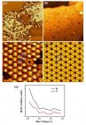
nanowerk亮点报道我实验室工作 10 月 1 日 , 纳米科技国际权威网站 nanowerk 亮点了郑之伟等人最近发表在美国光学学会 Optics Express 杂志 的工作 ( "Microwave and optical saturable absorption in graphene" ) ,题目是“石墨烯在微波光子学中崛起” ( The rise of graphene in microwave photonics ) 。郑之伟等人的这项工作利用实验室的光载无线通信系统( Radio-over-Fiber ) 从实验上发现石墨烯在微波和太赫兹波段的非线性可饱和吸收特性。之前,这一特性只在光频段被证实并被迅速应用于光电子器件中。郑之伟等人的工作开启了石墨 烯非线性可饱和吸收特性在微波和太赫兹光子学领域应用的大门,预计将在宽带无线接入网、高速微波信号处理、高速宽带调制器等方面发挥重要作用。 The rise of graphene in microwave photonics ( Nanowerk Spotlight ) In 2010, a Nanowerk Spotlight highlighted the importance of graphene in ultra-fast photonics and predicted that the unique energy band structure in graphene would allow it to actively respond to photons with ultra-wide spectrum range – from the visible to the infrared – with record strong inter-band transition efficiency. As expected, graphene based ultra-fast photonics has been rising fast in various aspects of ultra-fast photonics – an ultra-fast graphene photo-detector with bandwidth exceeding 500 GHz; a broadband graphene optical modulator; a broadband graphene polarizer etc, which all benefit from the material's broadband photonics property. Particularly, the optical saturable absorption in graphene, that is, optical absorbance of graphene, decreases with increasing light intensity and becomes saturated once the incident light exceeds a threshold power. This is a consequence of the Pauli blocking principle, which makes graphene widely applicable in the generation of different types of ultra-fast lasers at various wavelength from 1 µm to 10.6 µm. The increased focus on photonics with graphene has indeed refreshed conventional photonics research. Now, a Chinese graphene-photonics research team led by Professor Han Zhang and Shuangchun Wen at the College of Physics and Microelectronic Science, Hunan University, experimentally demonstrated for the first time that graphene – besides its well-known optical saturable absorption – also shows microwave and terahertz saturable absorption. These findings have been published in a recent edition of Optics Express ( "Microwave and optical saturable absorption in graphene" ) In the experiment, the researchers employed an optical frequency multiplication technique to produce the microwave signal around 100 GHz, also known as low-band THz wave. The millimeter-wave was generated, amplified, and delivered by a remote antenna, and detected by a Terahertz detector after reaching graphene samples. By adjusting the optical attenuator, which therefore makes the output microwave power widely adjustable, microwave transmittance in graphene can be measured under various microwave powers. Fig. 1: Experimental setup for 100 GHz microwave generation and characterization system of microwave saturable absorption in graphene. (Image: Dr. Zhang, Hunan University) The team also found that by continuously varying the microwave frequency from 96 GHz to 100 GHz, with a frequency interval of 0.8 GHz, microwave saturable absorption in graphene could be always identified, with a modulation depth of 4.58% ∼ 12.77%. By performing Z-scan measurement on the same sample, optical saturable absorption in graphene is also confirmed. Fig. 2. Microwave saturable absorption curve (on the left) and the Schematic of microwave saturable absorption in graphene (on the right). (Image: Dr. Zhang, Hunan University) This experiment demonstrates the broadband saturable absorption of graphene from optical band to microwave band. Based on its novel microwave property, Zhang and Wen anticipate that graphene may show potential applications in microwave photonics. Several novel microwave devices may result from this: 1) a graphene saturable absorber induced mode-locking or Q-switching of Microwave Amplification by Stimulation Emission of Radiation (MASER), like its optical saturable absorption property; 2) a graphene microwave modulator in which modulation levels can be manually controlled by tuning the Fermi level of graphene, similar to the structure of graphene-based broadband optical modulators; and 3) a broadband graphene polarizer at the microwave band, where microwave and graphene layers interact nonlinearly. Finally, Zhang and Wen summarize the possible advantages of graphene on microwave photonics devices: (i) tunable nonlinear microwave property through controlling the number of graphene layers or through chemical functionalization; (ii) facility to make graphene patterns at the millimeter scale by which more interesting microwave photonics phenomena may emerge; (iii) two-dimensional sheet structure makes it possible for microwaves to propagate either along the graphene surface or perpendicularly upon the graphene surface; (iv) small energy band gap in graphene which exactly matches with the photon energy of microwave and Terahertz photonics; (v) universal saturable absorption property indicates the mode-locking at the microwave band with frequency tunable operation. “At the current stage, research on graphene based microwave photonics is very limited but should be continuously rising” Zhang and Wen conclude. “This initial trial on the microwave photonics in graphene can be regarded as a starting point. The intrinsically small band gap and numerous Dirac points in graphene indicate that graphene may be a natural candidate material for microwave photonics because microwave photons exactly match with the small band gap in graphene. We believe that many new microwave photonic properties of graphene will be discovered and graphene could change the future of microwave communications – such as microwave signal processing, broad-band wireless access networks, sensor networks, radar, satellite communications, and so on.”
Digital Core Design , the world-famous design laboratory in Bytom, Poland, has developed the world’s first processor made of graphene – the BYT-ON. Discovered in 2004, graphene is an allotrope of carbon. Its structure is one-atom-thick planar sheets of carbon atoms that are densely packed in a honeycomb crystal lattice. Graphene differs from most conventional materials. Intrinsic graphene is a semi-metal or zero-gap semiconductor. The E-k relation is linear for low energies near the six corners of the two-dimensional hexagonal Brillouin zone, leading to zero effective mass for electrons and holes. Due to this linear dispersion relationship at low energies, electrons and holes near these six points behave like relativistic particles described by the Dirac equation for spin 1/2 particles. The end result is that graphene-based conductors can transport electronic signals at relativistic speeds, while graphene-based transistors can switch many orders of magnitude faster than their conventional silicon-based counterparts, all while consuming minimal power. In fact, graphene is such an amazing material that the Nobel Prize in Physics for 2010 was awarded to Andre Geim and Konstantin Novoselov at the University of Manchester "For groundbreaking experiments regarding the two-dimensional material graphene" . Use of graphene in Digital Core Design’ BYT-ON processor represents a breakthrough in electronics. The traditional silicon structure used to build conventional integrated circuits has been replaced with polycyclic aromatic hydrocarbons. “We commenced our tests just before the end of 2011, and the results far exceeded our expectations,” notes Tomasz Ćwienk, the spokesman for Digital Core Design. "We replaced the existing processor in one of the newest tablets available on the market with our graphene-based BYT-ON processor. We knew that the BYT-ON’s power-consumption was going to be minimal, but we were amazed to discover that the tablet ran all the way from the beginning of January 2012 until the end of March 2012– three full months – without our having to recharge the battery.” These revolutionary results were possible due to the combination of the Digital Core Design’s proprietary architecture (which is the outcome of 12 years of the company’s experience) and the graphene itself, which opens new possibilities for the electronic industry. The architecture implemented in the BYT-ON processor is called CISKoRISK 2nd Generation – it performs all operations with speeds reaching up 99.13% the speed of light, while maintaining 99.85% lower power consumption than conventional silicon-based equivalents. Editor’s Note: The rumor on the streets is that the world’s top ten FPGA vendors are already in secret consultations with Digital Core Design with regard to the application of the BYT-ON’s underlying graphene transistor structure as the basis for next-generation FPGAs. One tremendous advantage of this technology for FPGA applications is that memory cells (including configuration cells) constructed out of graphene transistors switch orders of magnitude faster than SRAM, have orders of magnitude higher density than DRAM, and the non-volatility of Flash, all while consuming almost zero power. Furthermore, graphene-based transistors are immune to radiation events, making this technology ideal for aerospace applications including deep-space probes. From: http://www.eetimes.com/electronics-blogs/pop-blog/4370188/BYT-ON---World-s-first-graphene-based-processor--graphene-based-FPGAs-to-follow-
发信人: buckyx (buckyx), 信区: NanoST 标 题: 石墨烯真的与众不同吗? 发信站: 水木社区 (Wed Dec 1 13:59:16 2010), 转信 终于有人出来泼冷水了。 ACS Nano上曾经有一篇石墨烯/二氧化钛复合材料的论文,认为复合之后的光催化活性强于二氧化钛和碳纳米管的复合材料。 刚刚ACS Nano又出来一篇同样内容的论文,题目很直接:Is TiO2-Graphene Truly Different from Other TiO2-Carbon Composite Materials? 这篇论文的表征更详细,认为在提高催化活性方面,石墨烯跟碳纳米管没什么大的差别。论文里说It is hoped that our current work could avert the misleading message to the readership ,文献37就是前面那篇论文。这两个工作都是国内的组做的。 客观的说,石墨烯和碳纳米管在提高性能方面到底有没有差别,也要取决于具体的材料,石墨烯和碳纳米管有很多种类,不同种类的性能肯定有差别。所以不能说上面两篇论文一个是对的另一个是错的。不过,像后面这一篇这样的论文还是挺给力的,尤其是在大家众口一辞说石墨烯怎么怎么好的时候。 发信人: Synthon (合成子信件请发给smartpolymer), 信区: NanoST 标 题: Re: 石墨烯真的与众不同吗? 发信站: 水木社区 (Wed Dec 1 14:34:04 2010), 转信 第一篇文章,graphene是氧化过的,CNT是没氧化的,这样solvothermal合成出来的复合物,跟TiO2的结合差别很大的。那个含氧基团留下的空位可以增进复合。我觉得没准换个氧化的CNT就跟graphene的性能差不多了。 第二篇文章,没有提供CNT样品制备的细节。。。
Monolayer Graphene as Saturable Absorber in Mode-locked Laser Authors: Qiaoliang Bao , Han Zhang , Zhenhua Ni , Yu Wang , Lakshminarayana Polavarapu , Kian Ping Loh , Zexiang Shen , Qing-Hua Xu , Ding Yuan Tang (Submitted on 14 Jul 2010) Abstract: We demonstrate that the intrinsic properties of monolayer graphene allow it to act as a more effective saturable absorber for mode-locking fiber lasers compared to multilayer graphene. The absorption of monolayer graphene can be saturated at lower excitation intensity compared to multilayer graphene, graphene with wrinkle-like defects, and functionalized graphene. Monolayer graphene has a remarkable large modulation depth of 95.3%, whereas the modulation depth of multilayer graphene is greatly reduced due to nonsaturable absorption and scattering loss. Picoseconds ultrafast laser pulse (1.23 ps) can be generated using monolayer graphene as saturable absorber. Due to the ultrafast relaxation time, larger modulation depth and lower scattering loss of monolayer graphene, it performs better than multilayer graphene in terms of pulse shaping ability, pulse stability and output energy. http://arxiv.org/abs/1007.2243
Vector dissipative solitons in graphene mode locked fiber lasers Han Zhang a , Dingyuan Tang a , , , Luming Zhao a , Qiaoliang Bao b and Kian Ping Loh b a School of Electrical and Electronic Engineering, Nanyang Technological University, Singapore 639798, Singapore b Department of Chemistry, National University of Singapore, Singapore 117543, Singapore Received 2 March 2010; revised 20 April 2010; accepted 21 April 2010. Available online 7 May 2010. Abstract Vector soliton operation of erbium-doped fiber lasers mode locked with atomic layer graphene was experimentally investigated. Either the polarization rotation or polarization locked vector dissipative solitons were experimentally obtained in a dispersion-managed cavity fiber laser with large net cavity dispersion, while in the anomalous dispersion cavity fiber laser, the phase locked nonlinear Schrdinger equation (NLSE) solitons and induced NLSE soliton were experimentally observed. The vector soliton operation of the fiber lasers unambiguously confirms the polarization insensitive saturable absorption of the atomic layer graphene when the light is incident perpendicular to its 2-dimentional (2D) atomic layer.
Original Paper Compact graphene mode-locked wavelength-tunable erbium-doped fiber lasers: from all anomalous dispersion to all normal dispersion H. Zhang 1 , D.Y. Tang * , L.M. Zhao 1 , Q.L. Bao 2 , K.P. Loh 2 , B. Lin 1 , S.C. Tjin 1 1 School of Electrical and Electronic Engineering, Nanyang Technological University, Singapore 639798, Singapore 2 Department of Chemistry, National University of Singapore, Singapore 117543, Singapore email: D.Y. Tang ( edytang@ntu.edu.sg ) * Correspondence to D.Y. Tang, 1 School of Electrical and Electronic Engineering, Nanyang Technological University, Singapore 639798, Singapore setDOI("ADOI=10.1002/lapl.201010025") Funded by: National Research Foundation of Singapore; Grant Number: NRF-G-CRP 2007-01 NRF-CRP Graphene Related Materials and Devices; Grant Number: R-143-000-360-281 Keywords fiber laser graphene mode-locked soliton nanophotonics Abstract Soliton operation and soliton wavelength tuning of erbium-doped fiber lasers mode locked with atomic layer graphene was experimentally investigated under various cavity dispersion conditions. It was shown that not only wide range soliton wavelength tuning but also soliton pulse width variation could be obtained in the fiber lasers. Our results show that the graphene mode locked erbium-doped fiber lasers provide a compact, user friendly and low cost wavelength tunable ultrashort pulse source. ( 2010 by Astro Ltd., Published exclusively by WILEY-VCH Verlag GmbH Co. KGaA) Compact graphene mode-locked wavelength-tunable er
国兴做出这个真不容易,很赞! http://www.rsc.org/Publishing/Journals/CC/article.asp?doi=b922733d Chem. Commun. , 2010, 46 , 3256 - 3258, DOI: 10.1039/b922733d Architecture of graphdiyne nanoscale films Guoxing Li, Yuliang Li, Huibiao Liu, Yanbing Guo, Yongjun Li and Daoben Zhu We have demonstrated a methodology to generate large area graphdiyne films with 3.61 cm 2 on the surface of copper via a cross-coupling reaction using hexaethynylbenzene. The device based on graphdiyne films for measurement of electrical property is fabricated and shows conductivity of 2.516 10 -4 S m -1 indicating a semiconductor property. PDF下载: Architecture of graphdiyne nanoscale films http://news.sciencenet.cn//htmlnews/2010/5/231845.shtm 作者:张巧玲 来源: 科学时报 发布时间:2010-5-7 9:15:52 选择字号: 小 中 大 我国科学家成功合成新的碳同素异形体 饱受重视的碳材料家族又诞生了一个新成员 最近,中科院化学所有机固体院重点实验室科研人员在国家自然科学基金委、科技部和中国科学院的资助下,在石墨炔研究方面取得了重要突破。研究人员利用六炔基苯在铜片的催化作用下发生偶联反应,成功地在铜片表面上通过化学方法合成了大面积碳的新的同素异形体石墨炔(graphdiyne)薄膜,研究结果发表在2010年的《化学通讯》( Chem. Commun )上。 据悉,近20年来,科学家们一直致力于发展新的方法合成新的碳同素异形体,探索其新的性能,先后发现了富勒烯、碳纳米管和石墨烯等新的碳同素异形体,并成为国际学术研究的前沿和热点,形成了交叉科学的独立研究领域。碳具有sp 3 、sp 2 和sp三种杂化态,通过不同杂化态可以形成多种碳的同素异形体,如通过sp 3 杂化可以形成金刚石,通过sp 3 与sp 2 杂化则可以形成碳纳米管、富勒烯和石墨烯等。由于sp杂化态形成的碳碳三键具有线性结构、无顺反异构体和高共轭等优点,人们一直渴望能获得有sp杂化态的新的碳同素异形体,并认为该类碳材料具备优异的电学、光学和光电性能而成为下一代新的电子和光电器件的关键材料。石墨炔是第一个以sp、sp 2 和sp 3 三种杂化态形成的新的碳同素异形体,最有可能被人工合成的非天然的碳同素异形体。 化学所有机固体院重点实验室科研人员长期致力于碳材料的合成、聚集态结构和性能的研究。他们成功研究出石墨炔薄膜后, Chem. Commun 的审稿人在评价这一研究成果时表示:这是碳化学的一个令人瞩目的进展,大面积的石墨炔薄膜的制备是一个真正的重大发现,研究结果非常让人振奋,并将为大面积石墨炔薄膜在纳米电子的应用开辟一条道路。 研究结果表明,石墨炔是由1,3-二炔键将苯环共轭连接形成二维平面网络结构的全碳分子,具有丰富的碳化学键,大的共轭体系、宽面间距(4.1913)、优良的化学稳定性和半导体性能。所获得的石墨炔薄膜面积可达3.61cm 2 ,是高晶化的单晶薄膜,拉曼光谱显示了其特征峰在1382、1569、1926和2189cm -1 ,并证实该薄膜具有较高的有序度和较低的缺陷,薄膜电导率为:10 -3 -10 -4 S m -1 。 这种新的碳同素异形体的发现,使得受国际科学界高度重视的碳材料家族又诞生了一个新的成员。石墨炔特殊的电子结构将在超导、电子、能源以及光电等领域具有潜在、重要的应用前景。 《科学时报》 (2010-5-7 A1 要闻) 更多阅读 《化学通讯》发表论文摘要(英文)
graphene_nature_photonics GRAPHENE Under high energy Appl. Phys. Lett. 96, 051122 (2010) Despite intense research into the preparation and characterization of graphene, there have been few studies into its suitability for applications in photonics. Graphene may have significant advantages over carbon nanotubes for ultrafast photonic applications, including a much lower level of saturable absorption, ultrafast recovery times (~200 fs) and a wide operating spectral range that covers the whole telecommunications band. Now, Yong-Won Song and colleagues from the Korea Institute of Science and Technology have used graphene as an intracavity passive power-modulating element, demonstrating efficient laser pulsation in the high-pulse-energy regime. The researchers have overcome the problem of optical power-induced thermal damage by ensuring evanescent field interaction between the propagating light and the graphene layer. The resulting passively mode-locked fibre laser has a central wavelength of 1,561.6 nm, a spectral width of 1.96 nm, a repetition rate of 6.99 MHz and an estimated pulse duration of 1.3 ps. These results suggest that graphene could be useful in ultrafast photonics.
Mode locking of Ceramic Nd: YAG with graphene as a saturable absorber The mode-locking of a ceramic Nd: YAG solid-state laser (SSL) with solution processed graphene as the saturable absorber (SA) was demonstrated. Transform-limited pulses of 4 ps with an average power of 100 mW centered at 1064 nm were generated, for a non-dispersion compensated Nd: YAG SSL. Z-scan studies revealed that the graphene SA had a saturation intensity of 0.87 MW cm -2 and a normalized modulation depth of 17 %. The results illustrate the potential of using graphene as a mode locker for SSLs. Appl. Phys. Lett. 96 , 031106(2010); doi:10.1063/1.3292018 Mode locking of Ceramic Nd: YAG with graphene as a
我们跟鲍师兄今年下半年才报道的石墨烯锁模的工作,11月就得到了曼彻斯特大学 物理学与天文学院的科斯特雅诺沃塞洛夫博士的关注 (见转载)。能引起石墨烯研究中心的科学家们的注意应该是对我们工作的一种肯定,所以倍感荣幸和挑战呀!不得不感叹石墨烯研究发展之迅速,世界资讯之发达。未来研究石墨烯在锁模激光器的应用也会越来越广,竞争自然会变得越来越激烈;不比一年前,只有 我们跟鲍师兄 暗地里做 石墨烯锁模 ,现在国际上相关的课题组都正在或者即将做石墨烯在超快激光中的应用;有几个课题组甚至还有文章即将发表。看来我们如果想保持领先地位,还必须继续创新,仍需继续努力呀!加油吧! 转载自: http://www.azonano.com/details.asp?ArticleId=2456 Graphene: From Physics to Applications Dr. Kostya S. Novoselov , School of Physics Astronomy , University of Manchester Corresponding author: kostya@manchester.ac.uk Graphene - one layer of carbon atoms arranged in a hexagonal lattice - is the newest member in the family of carbon allotropes. Although isolated graphene was reported for the first time only in 2004 1 , the progress it made over these years is enormous, and it rightly has been dubbed the wonder material. There are three major areas of excitement about graphene. Firstly, it is the first example of two-dimensional atomic crystal, which very existence improves our understanding about thermodynamic stability of low-dimensional systems. Secondly, the electronic properties of graphene are very peculiar: electrons in graphene obey linear dispersion relation (just like photons), thus mimicking massless relativistic particles 2 . And the last but not least, many properties of graphene are superior to those in all other materials, so it is very tempting to use it in a variety of applications, ranging from electronics to composite materials. Historically, it is the electronic properties which attracted most of attention. Electrons in graphene behave like massless relativistic particles, which governs most of its electronic properties. Probably one of the most spectacular consequences of such unusual dispersion relation is the observation of half-integer Quantum Hall Effect and the absence of localisation 2 . The later might be very important for graphene-based field effect transistors. Generally crystals of graphene could be prepared with very few defects (consequence of ultra strong carbon-carbon bonds), which, in conjunction with the absence of localisation and high Fermi velocity ensures very high mobility of the charge carriers and short time of flight in ballistic regime. First prototypes of high-frequency transistors have been recently developed and demonstrated very encouraging characteristics 3 . Also peculiar are graphene's optical properties. It has been measured that graphene absorbs 2.3% of light 4 - quite a sizable fraction for an ultimately thin material. What is even more exciting is the fact that this number is given solely by the combination of fundamental constants 4 : (=e 2 /hc1/137 is the fine structure constant). Do it at home, multiply 3.14 by 1/137 and you will get something close to 0.023. Such combination of high conductivity (sheet resistance of doped graphene can be as low as 10 Ohm) and low light adsorption makes this material an ideal candidate for transparent conductive coating. Graphene utilisation for this type of applications has been recently demonstrated by constructing graphene-based liquid crystal 5 and solar cells 6 . Furthermore, the general issue of graphene mass-production (until recently only research-size graphene samples have been available) has been resolved for these sort of applications with the introduction of a novel technique: large area thin films of micrometer-size graphene flakes can be produced by chemical exfoliation of graphite 5 . It is very tempting to use the unique properties of graphene for applications. The already mentioned examples do not even nearly exhaust the list of technologies which would benefit from using graphene. Composite materials and photodetectors, support for bio-objects in TEM and mode-lockers for ultrafast lasers - all those and many more areas would gain strongly from using graphene. The issue, however, was always the mass-production of this material. Since the very first experiments 1 , the technique of choice for graphene production for many researchers was the very nave Scotch-tape method 1 , 2 - simple peeling of graphene monolayers from bulk graphite with an adhesive tape. However, recent months seen a dramatic progress in development of truly mass-production techniques for graphene synthesis. Ranging from aforementioned chemical exfoliation to epitaxial growth (for a review see 7 ), these techniques give us a realistic hope that soon we will see products based on this exciting two-dimensional material. Reference 1. Novoselov, K. S., Geim, A. K., Morozov, S. V., Jiang, D., Zhang, Y., Dubonos, S. V., Grigorieva, I. V. Firsov, A. A. Electric Field Effect in Atomically Thin Carbon Films Science 306, 666-669 (2004). 2. Geim, A. K. Novoselov, K. S. The Rise of Graphene Nature Mater. 6, 183-191 (2007). 3. Yu-Ming Lin, Keith A. Jenkins, Alberto Valdes-Garcia, Joshua P. Small, Damon B. Farmer Phaedon Avouris, Operation of Graphene Transistors at Gigahertz Frequencies Nano Lett., 9 (1), 422-426 (2009). 4. R. R. Nair, P. Blake, A. N. Grigorenko, K. S. Novoselov, T. J. Booth, T. Stauber, N. M. R. Peres, A. K. Geim Fine Structure Constant Defines Visual Transparency of Graphene Science 320, 1308 (2008). 5. Peter Blake, Paul D. Brimicombe, Rahul R. Nair, Tim J. Booth, Da Jiang, Fred Schedin, Leonid A. Ponomarenko, Sergey V. Morozov, Helen F. Gleeson, Ernie W. Hill, Andre K. Geim, Kostya S. Novoselov Graphene-Based Liquid Crystal Device Nano Letters 8(6) 1704 - 1708 (2008). 6. X. Wang, L. Zhi, K. Mullen, Transparent, conductive graphene electrodes for dye-sensitized solar cells Nano Letters 8(1), 323-327 (2008) 7. A. K. Geim Graphene: Status and Prospects Science 324, 1530-1534 (2009). Copyright AZoNano.com, Dr. Kostya Novoselov (University of Manchester) Date Added: Nov 29, 2009
Applied Physics Letters , Vol. 95, pp. 141103. 原文下载 http://www3.ntu.edu.sg/home2006/ZHAN0174/apl.pdf Due to its unique electronic property and the Pauli blocking principle, atomic layer graphene possesses wavelength-independent ultrafast saturable absorption, which can be exploited for the ultrafast photonics application. Through chemical functionalization, a graphene-polymer nanocomposite membrane was fabricated and first used to mode lock a fiber laser. Stable mode locked solitons with 3 nJ pulse energy, 700 fs pulse width at the 1590 nm wavelength have been directly generated from the laser. We show that graphene-polymer nanocomposites could be an attractive saturable absorber for high power fiber laser mode locking.
石墨烯可以产生高能量超短脉冲 OPTICS EXPRESS,Vol. 17, P17630. http://www3.ntu.edu.sg/home2006/zhan0174/OE_graphene.pdf Abstract: We report on large energy pulse generation in an erbium-doped fiber laser passively mode-locked with atomic layer graphene. Stable mode locked pulses with single pulse energy up to 7.3 nJ and pulse width of 415 fs have been directly generated from the laser. Our results show that atomic layer graphene could be a promising saturable absorber for large energy mode locking.
石墨烯 (graphene)作为近年来的研究热点,有很多优异的物理性质。利用紧束缚方法(Tight-binding approach)计算出的能量色散关系(energy dispersion relation) 可以发现很多有趣的东西,同时对碳纳米管的研究也有一定的指导意义。 The energy dispersion relation formula. Honeycomb lattice and its Brillouin zone.( 以上公式和图见 Rev. Mod. Phys., Vol. 81,No. 1,109-162,2009 .) The values of Brillouin zone A number of interesting and peculiar features emerge from this figure. First it is clear that the valence and the conduction bands touch each other at a number of finite momentum values. The momentum values at which the two bands touch are termed Dirac points (there are two in the Brillouin zone) and are represented by the momentum vectors K and K’. As a consequence, graphene’s spectrum does not have an energy gap. On the other hand, since the bands only touch at two momentum points the density of states is zero at the corresponding energy. Therefore, grapheme is sometimes termed a zero-gap semiconductor with vanishing density of states at the Fermi energy.( J. Phys.: Condens. Matter 21 (2009) 323201 ) Dirac points附近的数值。 附Matlab程序 %单层石墨(graphene)的色散关系 %Copyright 2009 Zheng-Wei Zuo clc;clear all;close all %清除之前的内存空间变量、图形等 syms x y %d定义自变量,x代表Kx,以此类推; t=2.7;%the nearest-neighbor hopping energy (hopping between different sublattices). m=-0.2*t;%the next nearest-neighbor hopping energy (hopping in the same sublattices). a=1.42;%the carbon-carbon distance. E1=t*sqrt(3+2*cos(sqrt(3)*y*a)+4*cos(sqrt(3)/2*y*a)*cos(3/2*x*a))-m*(2*cos(sqrt(3)*y*a)+4*cos(sqrt(3)/2*y*a)*cos(3/2*x*a));%the upper band E2=-t*sqrt(3+2*cos(sqrt(3)*y*a)+4*cos(sqrt(3)/2*y*a)*cos(3/2*x*a))-m*(2*cos(sqrt(3)*y*a)+4*cos(sqrt(3)/2*y*a)*cos(3/2*x*a));%the lower band ezsurf(E1, )%plot the upper hold on %继续在当前图形上画图 ezsurf(E2, )%plot the lower shading interp; % 每个等高面用不同的颜色进行区分 box on%加外框 axis tight figure; %另外画一图形 ezsurf(E2, )%plot the upper hold on %继续在当前图形上画图 ezsurf(E1, )%plot the lower shading interp; % 每个等高面用不同的颜色进行区分 box on%加外框 axis tight
The first artificial graphene has been created at the NEST laboratory of the Italian Institute for the Physics of Matter (INFM-CNR) in Pisa. It is sculpted on the surface of a gallium-arsenide semiconductor, to which it grants the extraordinary properties of the original graphene. Published as a Rapid Communication on Phys.Rev.B, the research has been highlighted by the American Physical Society ( Engineering artificial graphene in a two-dimensional electron gas). They envisioned it at the NEST laboratory in Pisa (a joint INFM-CNR and Scuola Normale Superiore di Pisa lab), and then they sculpted it like a work of art on the surface of a gallium-arsenide semiconductor. They named it artificial graphene, the very first ever created, ready to raise the interests of both industry and research. This amazing copy promises to render available the incredible electronic qualities of graphene, and thus, it offers a way to overcome the closing physical limits that plague silicon. An exceptional result of Marco Gibertini, Achintya Singha, Marco Polini and Vittorio Pellegrini of INFM-CNR and Scuola Normale Superiore di Pisa, with the cooperation of Giovanni Vignale (University of Missouri), Aron Pinczuk (Columbia University) Loren Pfeiffer and Ken West (Alcatel-Lucents Bell Labs). 6 {2 O5 H8 e$ J: j, R2 w {; A0 W. @. @' M( m Natural graphene is an interesting but elusive material, observed for the first time in 2004. It has a very peculiar structure, being composed of a single layer of carbon atoms (only one atom thick) arranged in a grid which resambles common chicken wire. This structure grants graphene its exciting electronic properties: over this two-dimensional carbon nano world, electrons move almost freely at very high speeds, acting like massless p articles . For the electronic industry, this means more efficient devices that will be able to be built a lot smaller than what silicon allows. Such an innovation, however, is yet far away to come, because production of graphene with sizes and reproducibility needed by the semiconductor industry is not possible yet. 9 / J* c7 M - S* l( d V5 X V 9 @: K5 v# `jZ- ]1 ?. H And the idea proved to be a complete success: modified in this way, the nanosculptured semiconductor exhibits the properties of the famous material it imitates, thus becoming the very first artificial graphene. With an added advantage: the overall procedure does not rely on exotic equipments, but on tools and instruments that the nanofabrication industry already possesses and masters, meaning that the artificial graphene can already enable the development of high-mobility transistors and lasers. # I8 K/ |! a+ E; ?; ^! v' d1 | . F) M% [1 q6 L We are extremely happy commented Vittorio Pellegrini and Marco Polini to have been first in creating artificial graphene. This line of research has a great strategic importance, and for this reason very intense competition had sparkled between many research groups around the world. Being the first to create this material means in fact gaining a significant advantage in exploiting its extraordinary characteristics. And we believe that this artificial copy, already part of a semiconductor, may finally make graphenes properties available to be implemented in industrial projects and products. - w- B# J* [7 bv4 F) M8 H ( zg+ x# F( h' `! ~+ @ Source: National Institute for the Physics of the Matter
Applying innovative measurement techniques, research ers from the Georgia Institute of Technology and the National Institute of Standards and Technology have directly measured the unusual energy spectrum of graphene, a technologically promising, two-dimensional form of carbon that has tantalized and puzzled scientists since its discovery in 2004. Drawing represents a probe scanning and mapping the atomic contours of graphene, a single layer of carbon atoms arranged in a honeycomb-like array. Simultaneously applying a magnetic field causes electrons (ball) to organize in circular orbits, like a dog chasing its tail. Orbits hold clues to the materials exotic properties . Credit: Kubista, Georgia Institute of Technology. Published in this week's issue of Science , their work adds new detail to help explain the unusual physical phenomena and properties associated with graphene, a single layer of carbon atoms arrayed in a repeating, honeycomb-like arrangement. Graphene 's exotic behaviors present intriguing prospects for future technologies, including high-speed, graphene-based electronics that might replace today's silicon-based integrated circuits and other devices . Even at room temperature, electrons in graphene are more than 100 times more mobile than in silicon. Graphene apparently owes this enhanced mobility to the curious fact that its electrons and other carriers of electric charges behave as though they do not have mass. In conventional materials , the speed of electrons is related to their energy, but not in graphene. Although they do not approach the speed of light, the unbound electrons in graphene behave much like photons, massless p articles of light that also move at a speed independent of their energy. NIST-built STM shuttle module contains the atomic-scale position-and-scan system. Graphene sample and probe tip are in the center opening. Shuttle moves between a room-temperature vacuum environment for loading to an ultracold environment for measuring. Model in background shows graphene s honeycomb structure. Credit: Holmes, NIST This weird massless behavior is associated with other strangeness. When ordinary conductors are put in a strong magnetic field, charge carriers such as electrons begin moving in circular orbits that are constrained to discrete, equally spaced energy levels. In graphene these levels are known to be unevenly spaced because of the massless electrons. The Georgia Tech/NIST team tracked these massless electrons in action, using a specialized NIST instrument to zoom in on the graphene layer at a billion times magnification, tracking the electronic states while at the same time applying high magnetic fields. The custom-built, ultra-low-temperature and ultra-high-vacuum scanning tunneling microscope allowed them to sweep an adjustable magnetic field across graphene samples prepared at Georgia Tech, observing and mapping the peculiar non-uniform spacing among discrete energy levels that form when the material is exposed to magnetic fields. The team developed a high-resolution map of the distribution of energy levels in graphene. In contrast to metals and other conducting materials, where the distance from one energy peak to the next is uniformly equal, this spacing is uneven in graphene.The researchers also probed and spatially mapped graphene's hallmark zero energy state, a curious phenomenon where the material has no electrical carriers until a magnetic field is applied. The measurements also indicated that layers of graphene grown and then heated on a substrate of silicon-carbide behave as individual, isolated, two-dimensional sheets. On the basis of the results, the researchers suggest that graphene layers are uncoupled from adjacent layers because they stack in different rotational orientations. This finding may point the way to manufacturing methods for making large, uniform batches of graphene for a new carbon-based electronics. More information: D.L. Miller, K.D. Kubista, G.M. Rutter, M. Ruan, W.A. de Heer, P.N. First and J.A. Stroscio. Observing the quantization of zero mass carriers in graphene. Science. May 15, 2009. Source: National Institute of Standards and Technology.
 标签: graphene