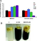
ElectrodepositedSulfur and Co x S Electrocatalyst onBuckypaper as High‑Performance Cathode for Li–S Batteries Yi Zhan, Andrea Buffa, Linghui Yu, Zhichuan J. Xu*, Daniel Mandler* Nano‑Micro Lett.(2020)12:141 https://doi.org/10.1007/s40820-020-00479-1 本文亮点 1. 硫活性物质和硫化钴催化剂被电沉积在碳纳米管巴基纸上,作为锂硫电池的 无粘结剂高性能正极 。 2. 多硫化物溶液的 电氧化成硫 和高活性硫化钴催化剂的 电沉积 显著地提高了锂硫电池正极制备的电流和时间效率。 内容简介 对具有更高能量密度的储能系统的日益增长的需求促进了对下一代先进可充电电池的研究。锂硫电池具有诱人的发展前景,硫正极的理论容量高达1675 mAh/g。但是锂硫电池存在数项技术挑战亟待解决,尤其是在硫正极上,包括硫的导电性差、充放电过程中的体积膨胀/缩小、多硫化物的穿梭效应等问题。耶路撒冷希伯来大学Daniel Mandler课题组联合南洋理工大学徐梽川课题组 通过简便的电沉积方法将硫和硫化钴(Co x S)电催化剂沉积在碳纳米管巴基纸(S/Co x S/BP)上,并用作电池的无粘合剂高性能正极。 通过多硫化物溶液( ~ S 6 2- ) 的电氧化将单质硫沉积在巴基纸上,这 种方法大大提高了制备硫正极的电流效率和时间效率。S/Co x S/BP正极在0.1 C时可提供高达1650 mAh/g 的初始放电容量,接近于硫正 极的理论容量;在0.5 C的电流速率下,S/Co x S/BP在第一个循环中的容量为1420 mAh/g ,在500个循环后的容量为715 mAh/g ,平均每个循环的容量衰减率为0.099%。 S/Co x S/BP的高容量可以归因于巴基纸中硫纳米颗粒的均匀分散和Co x S催化剂的存在。电沉积前用十二烷基硫酸钠(SDS)预处理巴基纸可以使其具有极性,易与多硫化物结合,因此有利于硫纳米颗粒在巴基纸中的良好分散。Co x S催化剂加速了多硫化物转化的动力学并减少了正极中多硫化物的存在,这抑制了多硫化物向锂负极的扩散,即穿梭效应。活性物质损失的减轻不仅改善了S/Co x S/BP的容量,而且还改善了其循环性。 图文导读 I 在巴基纸上电沉积硫(S/BP) 采用多硫化物电氧化法策略,在巴基纸碳纳米管表面原位沉积硫纳米颗粒,确保活性物质与电极紧密接触,参与电池反应。多硫化物的氧化还原是一个准可逆反应,反应速率较快且单质硫的高电阻引起的电位突变可以限制过厚的沉积物,控制硫的厚度。对从S/BP电极上取出的单个碳纳米管进行的EDS谱图表明,硫以薄层形式沉积在碳纳米管的表面上,且经过SDS处理的BP上硫的分布更加均匀。 图1. (a) 在20 mV/s扫描速率下10 mM多硫化物在BP电极上的CV;(b) 在10 mA cm -2 下BP电极上电沉积硫的计时电位法; (c) 在35 mAcm -2 下BP电极上电沉积硫的计时电位法; (d) S/BP单个纳米管的硫(绿色)和碳(红色)的EDS谱图; (e) 在S/BP-EtOH横截面的SEM图像上叠加EDS硫谱图; (f) 在S/BP横截面的SEM图像上叠加EDS硫谱图, BP的上侧对应于在沉积期间朝向对电极一侧。 经过SDS处理的S/BP可以提供高达1400 mAh/g的初始容量,而经过乙醇处理的S/BP-EtOH的初始容量大约为1197 mAh/g,表明S/BP的性能优于S/BP-EtOH。首次充放电后S/BP的硫晶型从α型转变为与S/BP-EtOH一样的β型,因此其优秀性能与晶型无关,主要源于其均匀的硫纳米颗粒分布。 图2. (a) S/BP的XRD谱图;(b) S/BP在0.1C倍率下的充放电曲线;(c) 首次充放电后S/BP和S/BP-EtOH的XRD图谱;(d) 在0.1 mV/s扫描速率下S/BP和S/BP-EtOH正极的CV。 II Co x S对多硫化物转化的电催化 为了进一步提高正极性能,通过电沉积在BP上制备了Co x S催化剂(Co x S/ BP)。由于非极性CNT对极性Co x S的亲和力较差,无定形Co x S纳米颗粒沉积在CNT的表面上并聚集。多硫化物在Co x S催化剂上表现出高可逆性,具有两对氧化还原峰,阳极峰位于0.47 V和0.25 V,相应的阴极峰位于-0.23 V和-0.46V。XPS光谱证实了在Co(II)/Co(III)氧化还原的帮助下,S 8 或长链多硫化物可形成S-S,从而在催化剂表面生成多硫酸盐配合物。 图3. (a) Co x S/BP,BP,Co x S300/BP和Co x S600/BP的XRD谱图;(b) Co x S/BP的TEM图像;(c) 在3 mV/s扫描速率下CoxS/BP电极在含/不含0.1 M Li 2 S 6 电解质的对称电池中的CV;(d) 使用不同温度退火的Co x S电极在对称电池中的CV。 图4. (a) 进行多硫化物催化之前的Co x S的XPS光谱;(b) 进行多硫化物催化之后的Co x S的XPS光谱。 III 在Co x S修饰的BP上电沉积硫(S/Co x S/BP) S/Co x S/BP在0.1C倍率下的首次充放电循环中可以提供高达1650 mAh/g的初始容量,接近硫正极容量的理论值。与S/BP和S/BP-EtOH相比,S/Co x S/BP在0.1、0.2、0.5、1和2 C时分别显示出1280、1190、1100、1030和950 mAh/g的最高容量,表明了Co x S通过催化多硫化物的转化,并有效减轻多硫化物的穿梭效应提高硫正极性能的优势。 图5. (a) S/Co x S/BP在0.1C倍率下的充放电曲线;(b) S/Co x S/BP、S/BP和S/BP-EtOH的倍率性能;(c) S/Co x S/BP在不同倍率下的充放电曲线;(d) 由充放电曲线得到不同电流密度下的充放电电位差。 在连续运行500个循环之后,S/ Co x S /BP仍拥有715 mAh/g的容量,平均每个循环的衰减率为0.099%,效率为~100%。当速率从0.5 C增加到1.0 C时,仍然可以保持良好的性能。S/ Co x S /BP的高性能不仅可以归因于SDS处理过的BP中电沉积的硫纳米颗粒的良好分散性,还可以归功于 Co x S 催化剂的存在促进了多硫化物转化的动力学。S/ Co x S /BP的良好循环稳定性还受益于 Co x S 的催化作用,该催化作用通过减少阴极上的多硫化物物种的积累而抑制了穿梭效应。 图6. (a) S/Co x S/BP、S/BP和S/BP-EtOH在0.5C下的循环性能;(b) S/Co x S/BP在不同条件下的循环性能。 作者简介 詹怡 本文第一作者 中山大学 副教授 ▍ 主要研究领域 电化学催化、纳米材料、电池技术 。 徐梽川 本文通讯作者 南洋理工大学 副教授 ▍ 主要研究领域 主要从事电化学基础、能源材料、能源转换和存储技术研究。 ▍ 主要研究成果 国际电化学学会会员,英国皇家化学会会员,美国电化学学会会员,Electrochimica Acta客座编辑,Clarivate Analytics,Web of Science高被引科学家(2018年和2019年)。 ▍ 课题组主页: https://www.ntu.edu.sg/home/xuzc/Research.html Daniel Mandler 本文通讯作者 耶路撒冷希伯来大学 教授 ▍ 主要研究领域 分 析物理,电化学,溶胶凝胶技术,薄膜和聚合物,医疗设备涂层和纳米技术 。 ▍ 主要研究成果 希伯来大学分析化学项目的负责人,发表 论文 200余篇,h指数为43。 ▍ 课题组主页: https://scholars.huji.ac.il/danielmandler 撰稿: 原文作者 编辑:《纳微快报》编辑部 关于我们 Nano-Micro Letters《纳微快报》是上海交通大学主办、Springer Nature合作开放获取(open-access)出版的英文学术期刊,主要报道纳米/微米尺度相关的高水平文章(research article, review, communication, commentary, perspective, letter, highlight, news, etc),包括微纳米材料的合成表征与性能及其在能源、催化、环境、传感、吸波、生物医学等领域的应用研究。已被SCI、EI、SCOPUS、DOAJ、CNKI、CSCD、知网、万方、维普等数据库收录。2019 JCR影响因子:12.264。在物理、材料、纳米三个领域均居Q1区(前15%)。2019 CiteScore:12.9,材料学科领域排名第4 (4/120)。中科院期刊分区:材料科学1区TOP期刊。全文免费下载阅读(http://springer.com/40820),欢迎关注和投稿。 E-mail: editor@nmletters.org Tel: 021-34207624
作为典型的一维纳米材料,碳纳米管具有优异的电学、力学和化学性质,因此在纳米电子器件、复合材料和催化剂等领域展现出了广阔的应用前景。目前,商业碳纳米管主要通过化学气相沉积法( CVD )制备。其原理是通过催化剂的作用裂解气相碳源,在基底上形成碳纳米管。然而传统的 CVD 法需要在制备过程中持续通入甲烷、乙醇等特定气体作为碳源,不仅大大增加成本,同时具有一定的安全隐患。因此,探索利用固体碳源制备碳纳米管逐渐成为近年来的研究热点。 最近,我们课题组在固体碳源制备碳纳米管的技术上取得突破,提出了一种低温下( 850 o C )利用固体碳源,通过 KOH 辅助原位气相沉积制备碳纳米管的新方法。该方法以普通固体生物质做碳源,并添加催化剂前驱体,在 800 o C 下进行初步石墨化,同时将催化剂( Ni )纳米颗粒均匀嵌入碳基体内部,形成石墨化碳与金属镍复合的中间体。在此基础上添加 KOH , 850 o C 下进行二次煅烧,在 KOH 与金属催化剂的作用下,发生碳的催化气化反应,持续释放含碳气体(如 CO 等),同时以此为碳源进行原位气相沉积,成功实现了从普通石墨化碳材料到碳纳米管的转变。其中碳纳米管的产率与添加 KOH 量相关。将所得材料用于超级电容器,表现出优于商业碳管 6 倍的比电容。该工作已发表在 Journalof Materials Chemistry A , 2016,4, 2137-2146,(相关链接: http://pubs.rsc.org/en/content/articlelanding/2016/ta/c5ta09631f ) 。该方法还可以拓展到多种固体碳源。
还有不到40小时,2013年就要过去了。在过去的一年里忙忙碌碌,很少静下来总结下自己的研究工作。上半年主要是集中精力写各种基金的申请书,做实验的时间被占用了不少。而下半年做实验的时间倒是增加了不少,但精力又被几篇修改的论文分去了一部分。 现在回头看看今年的一些科研工作,能够拿出来的也就下面三个工作: 1、采用低压空气电弧放电法成功实现了单壁、双壁、多壁碳纳米管的制备,尤其是双壁、多壁碳纳米管的宏量制备。单壁碳纳米管的大量制备还有一点难度,这将是2014年的重点科研课题。 2、采用热注射法制备了一系列无机量子点/石墨烯杂化物材料,初步研究了这些杂化材料的光电响应特性。正在投递和发表了若干篇相关的论文。这为我的碳纳米材料研究提供了新的应用方向。 3、将电弧放电法制备碳纳米管所产生的超细碳颗粒(副产物)进行分选,并以此为原料制备出碳量子点,详细研究了制备过程中反应温度、时间对碳量子点尺寸、光致发光特性的影响。研究证实了这种碳量子点具有很好地荧光上转换特性。 在过去的一年里以第1作者分别在Nanoscale、Mater. Res. Bull.上发表SCI论文3篇,以第2作者分别在Nanotechnology、Carbon、Mater. Lett.等国际SCI期刊上发表学术论文4篇。以第1发明人身份申请发明专利1项。另外有2项发明专利获得授权。另外,今年申请的几个基金中仅中了上海市自然基金,国家的青年基金评价为1A3B,会评没有通过。这使得我2014年申请基金的压力陡增!准备1月份把手头的工作暂且缓一下,全力准备基金申请。 2014年规划 基于2013年的科研状况,我2014年的重要工作也基本明确了,也就这么几点: 1、申请国家自然基金青年基金和教育部新教师基金 2、深入研究低压空气法大量制备单壁碳纳米管; 3、继续碳纳米材料及其应用研究; 4、适当提高论文发表档次。 2014年即将到来,希望我的2014能够一切顺利! 1. Y Su , X Lu, M Xie, H Geng, H Wei, Z Yang, Y Zhang. Nanoscale, 2013, 5(19), 8889–8893. 2. Y Su , H Wei, T Li, H Geng, Y Zhang. Mater. Res. Bull., 2014,50, 23–5. 3. Y Su , P Zhou, J Zhao, Z Yang, Y Zhang. Mater. Res. Bull., 2013, 48(9), 3232–3235. 4. Y Su , J Zhang; Lzhang, Y Zhang, J. Nanosci. Nanotechnol., 2013, 13, 1078–1081. 5. Y Su , M Xie, X Lu, H Wei, H Geng, Z Yang, Y Zhang, RSC Adv., Accepted. 6. H Wei, Y Su , Z Han, T Li, X Ren, Z Yang, L Wei, F Cong, Y Zhang. Nanotechnology, 2013, 24(23), 235706. 7. J Zhao, Y Su , Z Yang, L Wei, Y Wang, Y Zhang. Carbon, 2013, 58, 92–98. 8. H Geng, Y Su , H Wei, M Xu, L Wei, Z Yang, Y Zhang. Mater. Lett., 2013, 111, 204–207. 9. J Zhang, Y Su , H Wei, J Wang, C Zhang, J Zhao, Z Yang, M Xu, L Zhang, Y Zhang. Mater. Lett., 2013, 107, 251–254.
2013年9月Nature发表了Stanford大学研究组的文章,展示了世界上第一台基于碳纳米管的计算机的诞生。文章如下: M. Shulaker, G. Hills, N. Patil, H. Wei, H.-Y. Chen , H.-S. P. Wong , S. Mitra, “Carbon Nanotube Computer,” Nature , vol. 501, pp. 256 – 530, 2013. doi:10.1038/nature12502 Nature2013_The first CNT Computer.pdf 虽然这台碳基计算机的性能只能与1971年Intel发布的第一台微处理器Intel 4004相当,但这是发展以碳电子代替硅电子技术的重要的一步。 以下内容来源于IEEE Spectrum First Computer Made From Carbon Nanotubes Debuts By Rachel Courtland Posted 25 Sep 2013 | 17:00 GMT Share | Email | Print The days of silicon’s reign may be numbered. A team has built a computer using carbon nanotubes. The computer is rudimentary by modern standards: it contains just 178 carbon-nanotube-based transistors to the billions of silicon-based switches in modern chips. It operates on only 1 bit of information, where today we rely on 32- and 64-bit machines. And it clocks in at just 1 kHz, about a million times slower than the application processors we find in modern smartphones. Still, researchers say, the machine, developed at Stanford by a team led by professors H.-S. Philip Wong and Subhasish Mitra and described this week in Nature , is the first of its kind and an important step for a material that has long shown promise as an alternative to silicon. This is the first time that anybody has been able to put together a complete working computer based on any beyond-CMOS technology, says Naresh Shanbhag , a professor at the University of Illinois at Urbana-Champaign. (Shanbhag directs a chip research consortium called SONIC that includes Stanford University.) Researchers are hunting for an alternative to silicon because the transistor is no longer shrinking like it used to . The switches leak current, and the circuits based on them get hot. The problem is only going to get worse as transistors get smaller and circuits get denser. Carbon nanotubes , which are essentially rolled up, hollow sheets of carbon, have long shown promise as an alternative material. They are small, nanoscale structures that can theoretically be packed quite close together, and they exhibit very attractive electrical properties: current flows easily across them, and they can be switched on and off fairly easily. The first carbon nanotube transistors emerged in 1998 out of research groups based at IBM and Delft University of Technology . Since then researchers have succeeded in building smaller circuits, but developing very large scale integration (VLSI) processes that could be used to mass produce chips based on the material has been slow going. “Everybody wanted to build a commercial or large-scale digital system using these materials, but they could not do it because of the substantial imperfections that are inherent in carbon nanotubes,” says Mitra. There are two imperfections that have proved particularly problematic, say Mitra and his colleagues. One is that, although nanotubes can be grown fairly easily using chemical vapor deposition, the process tends to produce nanotubes with a mix of electrical properties: semiconducting and metallic. Metallic nanotubes are undesirable as they act as wires and can short out circuits. The other stumbling block is one of alignment. Carbon nanotubes can be grown on a pre-patterned wafer so they form parallel tubes. But a small fraction inevitably are misaligned, and can cut across and connect with neighbors. To make a process that could work in a commercial chip fab, the Stanford team developed a set of techniques they dub imperfection-immune design. They first eliminated the metallic nanotubes on their wafer by turning off all of the semiconducting nanotubes and driving a high current through the circuits. This caused the metallic nanotubes to overheat, oxidize, and ultimately vaporize into small puffs of carbon dioxide. The team then etched away sections of the mat of remaining nanotubes to form circuits. This etching was guided by an algorithm, based on graph theory, that can produce circuits that are mathematically guaranteed to work regardless of any imperfections, Mitra says, by cutting off at least part of any possible cross-cutting nanotube. The computer, built by graduate student Max Shulakar , isn’t one we’d recognize today. It uses only p-type metal-oxide-semiconductor (PMOS) logic. PMOS transistors are switched on when a negative voltage is applied. NMOS switches work with positive voltage. Although PMOS logic was the first to emerge in computing, today’s logic chips use both to make complementary (CMOS) logic. The disadvantage of PMOS is that it is effectively always on: it is a sort of network or resistors that relies on the presence of transistors of variable widths to regulate the flow of current and create voltage drops. But Shulaker and his colleagues show the computer is capable of everything you’d expect from a general purpose processor. It can run a basic operating system and multitask. It can perform counting and number sorting. They also demonstrate more modern silicon capabilities, by running 20 different instructions from the commercial MIPS instruction set. How does the computer work? It uses just one instruction to perform all computations: SUBNEG (subtract and branch if negative). As Franz Kreupl , a professor of electrical engineering at the University of Munich in Germany, writes in an accompanying commentary : SUBNEG takes the content of a first memory address, subtracts it from the content of a second memory address and stores the result in the second memory address. If the result of this subtraction is negative, it goes to a third memory address. Because the instruction contains this conditional statement, it guarantees Turing completeness -- that is, it can make any calculation if the computer has enough memory available. Rudimentary as the computer is, Kreupl says it is a notable advance in the hunt for silicon alternatives. The new work could do a lot to draw more attention to carbon nanotubes, which have lost the spotlight in recent years to graphene. “A circuit as complex as this one has never been devised,” Kreupl says. “I think it’s an important step forward.” There are of course, still a number of open questions. One is how well this approach will scale down. Working in an academic fab, the Stanford team was limited to an optical lithography resolution of just 1 micrometer, which limited the length of the carbon nanotubes transistors to about that distance (today silicon transistor dimensions are measured in the tens of nanometers). The density of the nanotubes patterned on the wafer was also low: just 5 per micrometer. That density would have to be boosted to 100 to 200 per micrometer, if not more, to increase speed and to make the process cost effective. Much progress will depend on how uniformly the transistors can be laid down. If the density varies too much, that would have an effect on the energy efficiency of the final circuit, Mitra says. There is work being done to address that issue. In the meantime, he says, we've reached a notable crossing point. People said you couldn’t build anything big with carbon nanotubes, he says. Now that question has been resolved.
《科学日报》( Science Daily) 2012 年 6 月 19 日 报道了在适当的温度条件下 , 采用适当催化剂 ,有可能 实现一个长 100cm , 比人头发细 5 万倍的完美单壁碳纳米管的形成。其实这项研究成果是美国赖斯大学机械工程与材料科学系的 Feng Ding 和 Boris I. Yakobson ,中国科学院上海技术物理研究所( Shanghai Institute for Technical Physics, Chinese Academy of Sciences )红外物理国家实验室的 Qinghong Yuan ,清华大学的 Zhiping Xu 以及香港理工大学的科研人员合作完成。此成果 2012 年 6 月 15 日 发表在《物理评论快报》网站—— Phys. Rev. Lett. 108, 245505 (2012) , Efficient Defect Healing in Catalytic Carbon Nanotube Growth. 摘要如下: The energetics of topological defects (TDs) in carbon nanotubes (CNTs) and their kinetic healing during the catalytic growth are explored theoretically. Our study indicates that, with the assistance of a metal catalyst, TDs formed during the addition of C atoms can be efficiently healed at the CNT-catalyst interface. Theoretically, a TD-free CNT wall with 10 8 –10 11 carbon atoms is achievable, and, as a consequence, the growth of perfect CNTs up to 0.1–100 cm long is possible since the linear density of a CNT is ~ 100 carbon atoms per nanometer. In addition, the calculation shows that, among catalysts most often used, Fe has the highest efficiency for defect healing.
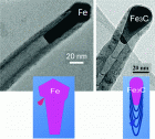
Iron Catalysts for the Growth of Carbon Nanofibers: Fe, Fe3C or Both? He et al. Chem. Mater. 2011, 23, 5379−5387 铁催化长出来的管子是直的 碳化铁催化长出来的管子是竹节状的 有意思。。。 Iron is a widely used catalyst for the growth of carbon nanotubes (CNTs) or carbon nanofibers (CNFs) by catalytic chemical vapor deposition. However, both Fe and Fe–C compounds (generally, Fe 3 C) have been found to catalyze the growth of CNTs/CNFs, and a comparison study of their respective catalytic activities is still missing. Furthermore, the control of the crystal structure of iron-based catalysts, that is α-Fe or Fe 3 C, is still a challenge, which not only obscures our understanding of the growth mechanisms of CNTs/CNFs, but also complicates subsequent procedures, such as the removal of catalysts for better industrial applications. Here, we show a partial control of the phase of iron catalysts (α-Fe or Fe 3 C), obtained by varying the growth temperatures during the synthesis of carbon-based nanofibers/nanotubes in a plasma-enhanced chemical vapor deposition reactor. We also show that the structure of CNFs originating from Fe 3 C is bamboo-type, while that of CNFs originating from Fe is not. Moreover, we directly compare the growth rates of carbon-based nanofibers/nanotubes during the same experiments and find that CNFs/CNTs grown by α-Fe nanoparticles are longer than CNFs grown from Fe 3 C nanoparticles. The influence of the type of catalyst on the growth of CNFs is analyzed and the corresponding possible growth mechanisms, based on the different phases of the catalysts, are discussed. Keywords: carbon nanotubes; carbon nanofibers; PECVD growth; Iron catalyst; α-Fe; Fe 3 C; growth mechanism; TEM
随着漫长的审稿,修改,辩论,我的关于在竹炭中利用其内部的硅酸钙生长碳纳米管的“大作”终于被Biomass Bioenergy接受了(网上可以查到了,也可以从点文件名pdf下载,不会侵权之类的吧)(Zhu J, et al., Synthesis of multiwalled carbon nanotubes from bamboo charcoal and the roles of .pdf , Biomass and Bioenergy (2011), http://dx.doi.org/10.1016/j.biombioe.2011.08.023 )。这篇文章可以说和常规的碳纳米管生长格格不入,是属于非典型的生长,典型的边缘研究方向。我简单介绍一下这个工作,或许有人感兴趣,同时也向那些在自己的研究方向上苦苦挣扎备受煎熬的研究生们,表示理解和鼓励。 熟悉碳纳米管的人都知道,生长碳纳米管早不是什么稀奇的事情,目前大家玩得花样都很新,可以说单纯的生长,已经勾不起人们的兴趣。我们的研究是误打误闯,走进这个生长领域的。在最初的时候,导师的想法是,复制生物结构得到同样结构的陶瓷,我们用的是竹炭,准备做碳化硅,事实上也做出来了,也发了一篇文章出来(Zhu JT, Kwong FL, Ng DHL. Synthesis of biomorphic SiCceramic from bamboo charcoal. J Nanosci Nanotechnol 2009;9(2):1564-7.)。大家都知道,做试验,如同炒菜,变着法的炒。有一次我朝炉子里通入TEOS(正硅酸乙酯),希望它能把硅源渗透到竹炭中去,然后使其反应得到碳化硅。在分析试验结果的时候,令我吃惊的是,长出来了很多的碳纳米管,多数的碳纳米管具有一个硅酸钙的头,里面填充了不少的硅酸钙,看起来很像那种VLS生长的模式。很感谢我的导师,他是一个很严谨的人,而且给学生足够的自由,他知道这个结果后,鼓励我深入研究,看看到底发生了什么事情。我本来就知道竹炭里是含有少量硅元素的,我就猜测,如果我直接加入纯净的炭源气体,会不会也有碳纳米管长出来呢,于是我试啊试啊,不过不出所料,竹炭里面的硅酸盐也能够生长碳纳米管。这期间,我还更换了新的试验炉管和气路管,避免出现样品的污染。不过得到的结果依旧是同样的。 大家都知道,常规的碳纳米管生长是需要金属做催化剂的,近年来利用半导体纳米粒子和金属氧化物纳米粒子也发现可以得到碳纳米管,可是利用化学盐(比如硅酸钙)来生长碳纳米管,听起来不那么可信,甚至有些那么点荒唐。是不是像六个手指挠痒,多一道子?很快就有老师质疑实验结果,因为竹炭本身是很有不少金属元素的,比如铁,那么这些铁到底参与了没有纳米管的生长呢?我们就用ICP-AES测定了竹炭里这些元素的含量,发现其实不多,(不过即使不多也可能参与了碳纳米管的生长),我又用XPS来测定生产物,发现铁的含量很低很低(至少在生长碳纳米管的位置),这也与在透射电镜里观察到的结果一致,没有铁的出现,只有硅酸钙! 这个工作是不是就可以得出结论,说硅酸钙是一种新的制备碳纳米管的催化剂呢?为了证明这一点,我就利用硅酸钙来作为催化剂直接制备碳纳米管,(这部分工作已经投到CARBON,审稿意见反响不错,正在修改),发现试验同样的结果。到此为止,我觉得是时候说硅酸钙可以作为催化剂制备碳纳米管了。 不过,肯定有人问,这个有什么意义?很了不起吗?说实话,这个问题困扰了我很久,对于自己这种非主流制备的碳纳米管,我很沮丧,也不知道会有什么用。终于有一天,遇见一个做地质的朋友,聊起这个,他竟然很感兴趣,原来他一直想向碳纳米管中填充硅酸盐,而我的碳纳米管在生长过程中便自己填充了硅酸盐。他说碳纳米管内部可以产生非常高的压强,和地球内部很深的地方压强等级,在碳纳米管里填充硅酸盐,就可以模拟地壳中硅酸盐的演变,进而对地球结构得到更多的了解,但是目前还没有相关报道,他试了很多次也成效不大。我听了非常兴奋,虽然不知道会不会真的像这位朋友说的那样,对他的研究有所帮助,不过还是觉得有一丝丝的安慰。 最后,感叹一句,这就是科学研究啊。 (同时恳请欢迎各位同行询问批评指正)
据美国《化学与工程新闻》( Chemical Engineering News )周刊March 17, 2011报道(DOI:10.1021/CEN030811072845)以碳纳米管为基础的饮水处理新系统,可以有效除去细菌和病毒,原文摘引如下: Nanotube-Based Filter Cleans Drinking Water Water Treatment: New filtration system removes bacteria and viruses Emily J. Gertz MICROBE ZAPPER When the carbon nanotube-based filter catches bacteria (left), it can also kill them through electrolysis (right). For 1 billion people in developing countries, finding clean drinking water is a daily challenge. Now researchers demonstrate a carbon nanotube-based filtration and electrolysis system that can completely remove or inactivate viruses and bacteria from water ( Environ. Sci. Technol. , DOI: 10.1021/es2000062 ). Coauthor Chad Vecitis of Harvard University thinks this technology could lead to inexpensive commercial water filters, potentially saving millions every year from diseases and death caused by waterborne pathogens. The key filter in the device is a porous film of multi-walled carbon nanotubes. Compared to other carbon-based filtration techniques, nanotubes have several advantages, Vecitis says, including large surface areas, inherent antimicrobial activity, and resistance to corrosion. By running a small current through the nanotubes and inserting another electrode into the water, the device also can electrolyze water to produce oxygen to kill pathogens. Vecitis and his colleagues tested their device by pumping suspensions of the bacteria Escherichia coli or of MS2 bacteriophages in a saline solution through the filter assembly. They ran these tests with and without electrolysis. After one pass through the filter, their device successfully removed all bacteria from the solution, and 99.99% of the viruses. With electrolysis, no viable bacteriophages remained. Since a single virus particle can sicken a person, the researchers consider electrolysis an important step. Because the electrolysis reaction requires low voltages, portable solar panels could power the device, Vecitis says. To adapt the technology to daily use, he says, the next step would be to create a more-compact device with the capacity to filter 2 to 3 L of water per day, the minimum people need to survive.
Chemical Engineering News M arch 11, 2011 A Better Way To Produce Organic Photovoltaics Materials Science: Researchers produce an all-carbon composite solar cell from organic components suspended in water Sarah Webb Jiaxing Huang STEALTH SURFACTANT Graphene oxide (GO) allows carbon nanotubes (SWCNTs) and fullerenes (C60) to form stable suspensions in water that researchers have used to build a photovoltaic device. Though solar energy surrounds us, scientists are still searching for the elusive combination of inexpensive materials and clean processing methods to harness that radiant energy cheaply. Now researchers have demonstrated that they can assemble an all-carbon, proof-of-concept photovoltaic cell by simply suspending the materials in water ( J. Am. Chem. Soc. , DOI: 10.1021/ja1103734 ). Engineers want to produce carbon-based photovoltaic cells because they would be cheaper, more flexible devices than those created with traditional inorganic materials such as silicon. But researchers struggle to manufacture carbon-based devices with the same solar efficiency as typical cells. Some of these inefficiencies stem from how researchers assemble the all-important layer that converts sunlight into electricity. In any photovoltaic cell, this layer must consist of materials that donate and accept electrons. For carbon-based systems, the electron-donating materials can be thin-walled carbon nanotubes and the electron accepting materials can be C60 fullerenes. But these materials tend not to disperse evenly, especially in water. To get the components to distribute so that they can then assemble in a thin layer, researchers either use reagents to covalently link electron donor to acceptor or mix in surfactants to help solubilize the two types of materials, which then can assemble into composite structures. Unfortunately, the covalent linkage method interferes with the flow of electrons in these surfaces. Meanwhile surfactants, which are insulators, find their way into the photovoltaic layer and disrupt charge transfer. Jiaxing Huang and his colleagues at Northwestern University thought graphene oxide could solve these issues. Last year, they showed that graphene oxide is a surfactant: though its surface is decorated with polar, oxygen-containing groups, it still contains greasy, hydrophobic patches ( J. Am. Chem. Soc. , DOI: 10.1021/ja102777p ). Unlike other surfactants, when reduced, graphene oxide produces an efficient conductor, graphene. Building on those findings, Huang and his colleagues mixed graphene oxide with C60 fullerenes and single-walled carbon nanotubes in water. They then sprayed an 8-nm-thick coat of this solution onto a glass slide and treated the surface with hydrazine to reduce the graphene oxide. The resulting surface was a smooth, all-carbon composite that integrates grapheme, the nanotubes, and fullerenes, Huang says. The team then made a proof-of-concept photovoltaic chip with this layer. These chips were up to 1,000 times more efficient at converting light into electricity than are similar organic devices developed with covalent chemistry, Huang says. The researchers now are improving those values by using fullerenes that absorb light more efficiently, such as C70, optimizing the graphene oxide reduction, and removing metallic impurities from the nanotubes. Edward Samulski of the University of North Carolina, Chapel Hill , says that before this method can become commercially viable, the researchers will need to show that they can control the nanoscale structure of the composite by adjusting the mixture of components. But by moving away from covalent linkages, he adds, the work is "a nice step" toward building more-efficient carbon-based photovoltaic devices. Related ACS Journals Surfactant-Free Water-Processable Photoconductive All-Carbon Composite J. Am. Chem. Soc. , DOI: 10.1021/ja1103734 Graphene Oxide Sheets at Interfaces J. Am. Chem. Soc. , DOI: 10.1021/ja102777p
这篇博文回忆一段往事,关于单壁碳纳米管的垂直定向生长,也关于一个实验室的迅速崛起。 纳米材料的定向化是一个科学问题。在纳米科学与技术这个多学科交叉领域,曾经有一个共同的目标,就是使纳米材料的本征性质在宏观尺度体现出来并付诸于应用。碳纳米管的学术价值主要体现在其独特的一维管状结构和众多优异的特性。如何将这些特性有机整合在一起组装成具有宏观尺寸的有序结构成了一个至关重要的问题。 回顾一下碳纳米管的发展史,会发现从无序到有序碳纳米管经历了一段相对漫长而曲折的历程,其中在两个重要的发展方向:定向化和连续化。定向化关注的是碳管或管束间的相对取向,从碳纳米管被发现算起经历了5年多的时间才得以实现 。国内的代表性工作有中科院解思深院士和清华大学范守善院士的早期工作,他们分别采用不同的方法实现了多壁碳纳米管阵列的垂直定向生长。这些工作深化了人们对碳纳米管的认识,极大推动了碳纳米管的后续应用。 同多壁碳纳米管相比,要实现单壁碳纳米管的垂直定向生长更加困难。因为单壁碳管直径更小(仅1 ~ 3 nm),要让如此细小的管状结构肩并肩排列垂直于基底生长不是一个简单的工作,对基底的表面、对催化剂尺寸和分布、对碳源的进给、对生长动力学的控制都有很高的要求。所以从1996年开始(或者更早),这个工作一直是这个领域最“给力”的方向。而经过了漫长的8年时间,直到2004年,还没有任何实质性的进展。 2003年我博士毕业后去日本筑波的产业技术综合研究所做博士后,在Suomio Iijima教授领导下的一个纳米中心做碳纳米管生长机制的研究。Iijima教授给我的任务是捕捉碳纳米管的形核点,找出碳管手性与催化剂晶体结构之间的关系。Iijima的这个中心当时共有三个小组,我在其中的“纳米检测组”,每天的工作很单调,就是在TEM铜微栅上直接生长碳纳米管,每次长几秒种,然后去看电镜。 由于经常在“合成组”做实验,在这里我认识了Kenji Hata。当时Hata刚从美国哈佛大学做完博士后,回到日本工作。他在美国的合作导师是Charles M. Lieber,所以在聊天时经常会有“想当年兄弟我在哈佛时...”这样的语气。但他碳纳米管的背景不强,起码在当时我感觉他还是一个菜鸟。正因为如此,他随后几年的迅猛发展才让我大为震撼。 Hata是从“一穷二白”开始起步的。当时他要做的事情很简单:就是把单壁碳纳米管从无到有制备出来。方法借鉴自他在哈佛时的一位同事 :将硅片在硝酸铁溶液里浸沾来获取催化剂,然后以乙烯做碳源在700摄氏度长碳管。做了几个月没有效果。他还尝试了快速加热、电场定向等方法,结果都不理想。记得那时哪怕获得一张好看一点儿的SEM图或Raman谱,他都兴奋得给整个中心发邮件。 2004年,日本东京大学的Maruyama小组在单壁碳纳米管定向生长上取得突破性进展。他们采用简单的浸沾法在石英片上均匀沉积上一层致密的Co/Mo双催化剂,以酒精为碳源,首次实现了定向单壁碳纳米管阵列的垂直生长,非常好的工作。只可惜这个工作并没有发到Nature/Science一类顶级期刊上,而是发表在平平的Chemical Physics Letters 以及后来的Optics Letters和Carbon上 。 Hata随后邀请Maruyama教授到筑波访问交流。不清楚是不是Maruyama的这次来访给Hata带来了好运。反正自那以后,Hata的人品爆发了,他意识到碳纳米管生长过程中催化剂与碳源的匹配关系,并注意到酒精中有氧,从而想到在碳源中通入同样含氧的水,是否也能促进碳纳米管的生长。他放弃了浸沾法,选择溅射法沉积催化剂,并在硅片和催化剂间预沉积了一层Al2O3缓冲层。他开始玩命地做实验,有时在clean room一呆就是一宿。但此君生活其实很有规律,每天下午4:00都能看到他出去锻炼,带着耳机围着研究所跑圈,一身热汗回来后接着做实验。 说到Hata,不能不提到另外一位仁兄:Don Futaba。此君系美日混血,在美国时和Hata相识,后来到日本工作。身上有日本人的严谨,也有美国人的顽皮。有时在路上老远就看到他藏在角落里,等你经过时故意从旁边闪出来吓你一跳,然后装作路过的样子走开。但每次我去他们实验室,都看到他一动不动坐在CVD炉旁边,耐心地等着炉子升温、降温。有一次聊起碳纳米管的生长,他故作神秘地左右瞧瞧,然后压低声音对我说:“The secret is water...”。 也是从那时候开始,他们实验室里的炉子和气路变得越来越复杂,最开始只有两三台CVD炉,不到一年的时间,整个屋子里就推满了炉子、真空装置、AFM、溅射仪等,管路纵横交错如麻,让人眼花缭乱。 2004年8月,我离开日本前往美国,期间获悉他们的进展神速。2004年11月,他们的题为“Water-Assisted Highly Efficient Synthesis of Impurity-Free Single-Walled Carbon Nanotubes”的文章在Science上发表 ,主要贡献就是在碳纳米管生长过程中引入微量水分做为弱氧化剂,刻蚀非晶碳,从而保持催化剂的活性,以促进碳管快速生长,形成定向垂直阵列。他们后来将这种方法命名为“Super growth”。接下来,他们的工作一发不可收拾,先后实现了双壁碳纳米管的定向生长、碳纳米管阵列在金属衬底上的生长,以此为基础开发了超级电容器电极材料、微机电器件,揭示了碳纳米管的超粘弹性等 。 我一直将Hata小组的迅速崛起看作是成功科研模式的一个经典范例,其中有很多东西值得我们学习:耐得寂寞、善于合作、抓住机遇、大胆构想、勤奋... 自2004年以来,多种单壁碳纳米管阵列制备工艺被先后开发出来,包括CO-CVD、氧气CVD、微波等离子增强CVD、热丝CVD、氨气CVD等 。其中让人钦佩的是戴宏杰小组的氧气CVD法,他们竟然直接将氧气和氢气混合来达到促进碳管生长的目的!敢这么做是需要胆识的。 参考文献: W. Z. Li, et al. Science 274, 1701 (1996). M. Terrones, et al. Nature , 388, 52 (1997). Z. F. Ren, et al. Science 282, 1105 (1998). S. S. Fan, et al. Science 283, 512 (1999). J. H. Hafner, et al. J. Phys. Chem. B 105, 743 (2001). Y. Murakami, et al. Chem. Phys. Lett. 385, 298 (2004). S. Maruyama, et al. Chem. Phys. Lett. 403, 320 (2005); S. Yoo, et al. Optics Lett. 30, 3201 (2005); S. Noda, et al. Carbon 44, 1414 (2006). K. Hata, D. N. Futaba, K. Mizuno, T. Namai, M. Yumura and S. Iijima, Science 306, 1362 (2004). D. N. Futaba, et al. Phys. Rev. Lett. 95, 056104 (2005); D. N. Futaba, et al. Nature Mater. 5, 987 (2006); T. Hiraoka, et al. J. Am. Chem. Soc. 128, 13338 (2006); T. Yamada, et al. Nature Nanotechnol. 1, 131 (2006); Y. Hayamizu, et al. Nature Nanotechnol. 3, 289 (2008); M. Xu, et al. Science 330, 1364 (2010). L. Zhang, et al. Chem. Phys. Lett. 422, 198 (2006); G. Y. Zhang, et al. PNAS 102, 16141 (2005); G. F. Zhong, et al. Chem. Vapor Deposition 11, 127 (2005); T. Iwasaki, et al. J. Phys. Chem. B 109, 19556 (2005); G. F. Zhong, et al. Jpn. J. Appl. Phys. 44, 1558 (2005); G. F. Zhong, et al. J. Phys. Chem. B 111, 1907 (2007); Y. Q. Xu, et al. J. Am. Chem. Soc. 128, 6560 (2006); M. Cantoro, et al. Nano Lett. 6, 1107 (2006).
2001年4月5日,Science在网上抛出了一篇重磅paper,单是题目就让搞碳纳米管的诸君为之一振:Single Crystals of Single-Walled Carbon Nanotubes Formed by Self-Assembly 。文章说的是以C 60 和Ni为原料,在真空和磁场作用下,在Mo衬底上合成了碳纳米管单晶。 何为碳纳米管单晶?给个简单的定义:在宏观尺度下可见、可操纵的,由单一手性的单壁碳纳米管以六边形点阵定向密排构成的晶体结构。此前的碳纳米管管束(Bundles)直径不过几十至几百纳米,而该文号称获得了微米尺寸的单晶体,并给出了完备的表征数据,包括EELS、TEM和电子衍射(图1)。文章的通讯作者是IBM苏黎士实验室(Zurich Research Laboratory)的J. K. Gimzewski,彼时已到加利福尼亚洛杉矶分校(University of California at Los Angeles)任教。 图1 碳纳米管单晶的合成示意图、电子衍射谱和TEM图像 Gimzewski也深以此工作为豪,以迅雷不及掩耳盗铃之势申请了专利,并在网上专设一主页宣传这项工作(如今这主页的链接已无处查询,以下是当时我存留的图片和文字): NANOTUBE MONOLITH DISCOVERY 2001 The monolith appears and provides the man-apes with the knowledge necessary to create new tools Technological advances are driven by tools The monolith appears again in 2001: The material from space in the lab; A Nanotube Crystal 这个工作意义非同小可,如果一旦获批量生产,则碳纳米管全面走入实际应用指日可待。2002年底我开始写博士论文时,满怀崇敬之心将这篇文章列在我的第1章文献综述中,并加以详细描述。孰知天有不测风云,2003年5月23日Science上发出了一篇对 文的Technical Comment ,指出Gimzewski的实验有误。提出质疑的是美国橡树岭国家实验室(Oak Ridge National Laboratory)的David B. Geohegan和莱斯大学(Rice University)的Richard E. Smalley(1996年诺贝尔化学奖获得者,C 60 的发现者之一,碳纳米管超级无敌大专家)等人。这几位当年也因对 文的工作颇感膜拜,遂立了项开始大张话旗鼓准备重现此结果,花了两年时间,却得到了一个让人大跃眼镜的结论,原文得到的单晶其实是含Mo的纳米棒或微米棒,电镜图像和电子衍射图谱均来自这个东东而非碳纳米管。铁证在前,Gimzewski等人只得最终承认:..., we accept that our conclusion of the growth of single crystals containing SWCNTs was mistaken 。好在那时我虽已通过答辩,论文还未上交图书馆,立马将这一段从论文第1章中删除,否则就要闹一个笑话。当时非典在北京肆虐,也没有这般紧张。 只是Gimzewski似乎并未完全认错,以他为第一发明人的美国专利于2004年公开,如今已经正式授权(Crystals comprising single-walled carbon nanotubes, US 6800369)。看来他要将错就错了。 碳纳米管单晶至今仍没有在实验上被成功合成。每每忆起这段历史,都是一声叹息。众所周知,碳纳米管的独特之处在于其结构的多样化。手性不同的单壁碳纳米管会呈现出截然不同的性能。因具有不同的能带结构,它们可呈金属性或半导体性;而半导体性碳管又因能隙不同而具有不同的电学和光学性能。试想,有几块碳纳米管单晶摆在你的面前,它们因为所含碳管手性的不同而具有不同的能隙,由于对不同波长可见光的吸收而呈现五彩斑斓的颜色(图2);它们可被加工,可被组合。实用而又高贵;赏心而又悦目。取代硅也仅是其众多应用之一而已。 图2 碳纳米管单晶结构示意图 曾经一直以为,碳纳米管单晶合成之日,就是Iijima获诺贝尔奖之时。如今看来,谁得奖谁不得奖,该做什么还得做下去。当年Geim因为不忿碳纳米管,心想你们都跟风赶时髦,我单剑走偏锋,把碳纳米管刨膛开肚做石墨烯。虽然最开始文章投Nature被拒,申请基金不批,最终还是发了Science,从此一路顺畅。正当诸君还在琢磨石墨烯时,人家又弄出个更广义的Two-dimensional atomic crystals ,除了石墨之外,随便把两个晶体在一起蹭一蹭,就得到了相应的单层二维结构。接着又在石墨烯上引入氢原子,搞出个石墨烷(Graphane) 。如今,原来做碳纳米管的诸君都开始做石墨烯了,做石墨烯的也就该换个思路了。 后注:与碳纳米管单晶合成最接近的工作是日本产业技术综合研究所Hata小组的液体凝聚法 和中科院物理所解思深院士和国家纳米中心孙连峰研究员的金刚石拉丝模法 ,都可使单壁碳纳米管紧密排列成定向规则结构,但仍无法对碳管的直径和手性进行精确控制。 参考文献: R. R. Schlittler, et al. Science, 2001, 292, 1136. M. F. Chisholm, et al. Science, 2003, 300, 1236. K. S. Novoselov, et al. PNAS, 2005, 102, 10451. D. C. Elias, et al. Science, 2009, 323, 610. D. N. Futaba, et al. Nature Mater., 2006, 5, 987. G. T. Liu, et al. Nano Lett., 2008, 8, 1071.
2010年10月4日,诺贝尔物理学奖揭晓,获奖者是英国曼彻斯特大学物理和天文学院的Andre Geim和Konstantin Novoselov,获奖理由为二维空间材料石墨烯(graphene)方面的开创性实验。从2004年石墨烯被成功剥离 至2010年斩获诺贝尔奖,是什么魔力让这一看似普通的碳材料在短短的6年时间内缔造了一个传奇神话?而回眸看其同族兄弟碳纳米管,自1991年被发现至今近20年,历经风雨,几经沉浮,不过是为他人做嫁衣裳。 石墨烯即为单层石墨片,是构成石墨的基本结构单元;而碳纳米管是由石墨烯卷曲而成的圆筒结构(图1)。作为一维(1D)和二维(2D)纳米材料的代表者,二者在结构和性能上具有互补性。从结构上来看,碳纳米管是碳的一维晶体结构;而石墨烯仅由单碳原子层构成,是真正意义上的二维晶体结构。从性能上来看,石墨烯具有可与碳纳米管相媲美或更优异的特性,例如高电导率和热导率、高载流子迁移率、自由的电子移动空间、高强度和刚度等。网上大多溢美之词:Pencil + sticky tape = desktop supercollider + post-silicon processors,Material of the Future,A thoroughbred that has to be tamed,Electron superhighway,...。目前,关于碳纳米管的研究,无论在制备技术、性能表征及应用探索等方面都已经达到了一定的深度和广度。组成及结构上的紧密联系,使二者在研究方法上具有许多相通之处。事实上,很多针对石墨烯的研究最开始都是受到碳纳米管相关研究的启发而开展起来的。 图1 石墨烯与碳纳米管 石墨烯的发展历程与碳纳米管极为类似。在碳纳米管被发现之前,碳的晶体结构主要有三种:石墨、金刚石和富勒烯(以C 60 为代表 )。当时,对于碳纤维(已工业化应用)和碳纳米纤维都已经有了很充分的研究;在碳纳米管被发现 之后,人们开始关注碳纳米管与碳纳米纤维之间的异同。从表面上看,在晶体结构上,碳纳米纤维的晶化程度相对较差,缺陷较多,石墨层片排列不连续,直径较大,并不真正属于碳的晶体结构,或者仅算是石墨的一种衍生物。如果单从这一点来看,碳纳米管的出现似乎仅是碳纳米纤维的一个延伸。因此,很有一些人并不把碳纳米管的发现归功于Sumio Iijima。事实上,碳纳米管的发现意义体现在人类观念的更新,标志着对碳晶体结构(甚至整个碳范式)有了更为深入的认识,是本质上迈进的一大步。尤其是单壁碳纳米管、双壁和薄壁碳纳米管的可控合成为充分认识碳纳米管的性能奠定了坚实的实验基础。值得一提的是,一些制备碳纳米管的方法大都借鉴自碳纳米纤维(如化学气相沉积法)。在一些早期研究中,对碳纳米纤维和碳纳米管的区分并不十分严格。对比石墨烯与碳纳米管(图2),可显见类似的发展轨迹。在石墨烯在实验上被发现之前,一些微小石墨晶粒、晶须或石墨层片(层数较多)就已经被合成出来并被广泛研究。膨胀石墨也是基于剥离石墨的理念,相关技术发展纯熟,工业化应用已久。同单壁、双壁、薄壁碳纳米管之间的关系类似,除了严格意义上的石墨烯(单层)外,双层和少数层石墨层片在结构和性能上也都明显区别于块体石墨,在广义上也被归为石墨烯的范畴。 图2 石墨烯与碳纳米管的发展历程 虽然石墨烯与碳纳米管有着类似的前生,却很可能拥有不一样的未来。原因有多方面,但最终可归结为一维材料与二维材料之争。纳米线、纳米管在同薄膜材料的较量中往往处于劣势。以碳纳米管为例,单根碳纳米管可被视作一根具有高长径比的单晶,但目前的合成和组装技术还无法获得具有宏观尺寸的碳纳米管晶体(将在后文中详述),从而限制了碳纳米管的应用。石墨烯的优势在于本身即为二维晶体结构,具有几项破纪录的性能(强度、导电、导热),可实现大面积连续生长,将Bottom-up和Top-down结合起来,未来应用前景光明。另外,石墨烯是量变引起质变哲学思想的典型范例。石墨烯更受物理学家的青睐,是进行科学实验、解决科学问题的理想平台,这也是促成其本次获奖的主要因素。碳纳米管地位尴尬,不可能给物理奖,给个化学奖也不太像,何况已有C 60 在先。 后注:石墨烯作为石墨(及后来的碳纳米管)的基本结构单元在理论上已被研究长达60余年 。在Geim和Novoselov的工作之前,薄层石墨已有多处报道。例如,哥仑比亚大学(Columbia University)的Philip Kim 和德克萨斯大学澳斯汀分校(University of Texas at Austin)的Rodney Rouff (当时在Washington University)都曾对石墨剥离薄层石墨片进行过研究,很可惜未得到单层石墨烯。 参考文献: K. S. Novoselov, et al. Science, 2004, 306, 666. H. W. Kroto, et al. Nature, 1985, 318, 162. S. Iijima. Nature, 1991, 354, 56. P. R. Wallace. Physical Review, 1947, 71, 622. A. K. Geim, P. Kim. Scientific American, 2008, 4, 90. X. K. Lu, et al. Nanotechnology, 1999, 10, 269; Applied Physics Letters, 1999, 75, 193.
CNTs are now longer and faster Scientists in China have grown carbon nanotubes to record-breaking lengths of 20 cm using a method that is faster and more efficient than previous techniques. Fei Wei, Weizhong Qian and colleagues from Tsinghua University and the Chinese Academy of Sciences in Beijing, China, have now modified this technique to produce longer tubes more quickly. The scientists are now trying to make even longer tubes for use as super-strong fibers; they also hope to use the nanotube to make transistor devices. 原文请参考: http://www.natureasia.com/asia-materials/highlight.php?id=664utm_source=NPG+Asia+Materialsutm_content=Research+Highlights http://pubs.acs.org/doi/abs/10.1021/cm903866z
据美国物理学家组织网报道,美国耶鲁大学的工程师们发现,碳纳米管上的缺口可促使 T 细胞(一种白细胞)抗原在血液中聚集,并激发人体自身的免疫反应,从而改进目前常用的继承性免疫疗法,有效增强病患的抗癌能力。相关研究发布在 4 月 20 日出版的美国《朗缪尔》( Langmuir )杂志上。 继承性免疫疗法,又称细胞转移疗法,是指从患者体内的免疫系统中提取细胞,对其进行改良,使之更有效地针对患者的特定病症,随后把它们重新注入患者的免疫系统,以攻击诱发疾病的相应细胞。虽然人体自身也会产生抗肿瘤的 T 细胞,但其经常会被肿瘤所 压制 ,且有效的细胞数量也十分有限。而采用体外培植的方式可有效保证 T 细胞的数量和质量,达到更好的抗癌效果。 研究小组之前也曾报告过碳纳米管对于增殖 T 细胞的意外效果。他们发现,当抗原的总数一定时,把碳纳米管制成的 外衣 附在抗原的表面,可使 T 细胞的增殖速率远高于抗原被聚苯乙烯等材质制成的薄膜包裹时的培植速度。这是由于抗原能够在碳纳米管的 缺口处 聚集,从而达到较好的增殖效果。 论文的主要作者、耶鲁大学化学工程和生物医学工程系的副教授塔瑞克 法米表示,碳纳米管束和淋巴结的微环境相似,具有复杂的几何结构,其可以模拟生理学吸收更多的抗原,激发更强烈的免疫反应。将碳纳米管用于人体的传统方法能够引起栓塞等问题,但将碳纳米管放入血液内培植细胞时,却不涉及将其植入体内,因此并不存在类似问题。 实验数据表明,继承性免疫疗法需要花费数周才能生成足够的 T 细胞,而碳纳米管在三分之一的时间内就能生成与继承性免疫疗法同等数量的细胞。研究人员表示,这是探索碳纳米管独特性质的一种新方式,也是碳纳米管在生物领域安全应用的一次创新。下一步,研究团队将着手探索更为有效的、将碳纳米管从血液中移除的方式,随后再将血液重新输回病患体内。(
纳米器件的设计与研究方兴未艾,如何为纳米器件提供一个纳米级的磁场,似乎并不是一件容易的事。如采用纳米永磁材料,一方面受到超顺磁尺寸的限制,另一方面磁场的强度是固定的,无法根据需要调变磁场强度。采用螺旋管提供电磁场可能是比较好的方法,磁场强度可以根据电流大小来调控,但是如何得到纳米级的螺旋管?用传统材料绕制是不可能的。螺旋碳纳米管(或螺旋碳纳米纤维)可能是一个比较好的选择。 与直线型的碳纳米管相比,螺旋碳纳米管可以用来做纳米级电磁铁,而磁场的强度可以用通过碳纳米管的电流来调节。下图是我们采用CVD原位催化裂解的方法制备的碳纳米弹簧SEM照片。 最近我们采用原位催化CVD方法,通过改变反应条件,合成了各种形态的碳纳米材料,如螺旋碳纳米纤维,纳米球链,碳纳米带等。下图是碳纳米带SEM和TEM照片: 由于制备这些碳纳米材料所用的催化剂为原位合成的纳米级过渡金属颗粒,因此所得到的复合物具有磁性。研究表明它们的微波吸收性能很好,且比重小,性能稳定,有望用于轻质隐身材料。 相关研究工作发表在以下刊物: 1. X.S. Qi, W. Zhong* , et al ., Carbon , 48, 365 (2010) 2. Xiaosi Qi,Yu Deng, Wei Zhong,* et al. , J. Phys. Chem. C 114 , 808 (2010) 3. X.S. Qi, M.H. Xu, W. Zhong* , et al , J. Phys. Chem. C 113, 2267 (2009) 4. Xiaosi Qi, Wei Zhong,* et al. , J. Phys. Chem. C 113 , 15934 (2009) 5. Xiaosi Qi, Yi Yang, Wei Zhong* , et al. , J. Solid State Chem. 182, 2691 (2009)
化学工程与碳纳米管:我们的坚守 看到林峰的博文,《 纳米是灌水领域吗? 》,以及李永丹老师的博文,《 负重登山的化工应用基础研究 》。看过之后,想说点自己的想法。 李永丹老师的文章说的很清楚,目前化学工程方面的研究处在一个很尴尬的地位。一方面,老牌的化工期刊影响力不够,而且不够与时俱进,为我们的领导们所不屑。所以,相当多的人,被迫在相关的学科里头寻找机会,比如纳米,就是一个机会。用我老板的话来说,research has its fashion, and we have to follow the fashion。 于是经常有人会问我,你看你们化工系的人,现在也有这么多人做纳米,那你们跟搞纳米化学、纳米材料、纳米物理的人有什么区别呢? 区别就在于,我们还是化学工程师,我们还希望坚守我们的一些原则,我们的思维方式和研究方法。 比如碳纳米管,这个东西是材料科学家们首先给折腾出来的,然后化学家们开始研究它的合成,物理学家们开始研究其中的物理现象,在物理学家和电子工程专家的共同努力下,貌似现在在某些场合有很不错的潜在应用。 但是如果我们不能够大规模的生产碳纳米管,那么这些潜在应用,始终只能停留在潜在的阶段。但是遗憾的是,化学家们认为他们已经阐明的碳纳米管生产的过程,现在剩下的工作,就是如何研究它的应用。其他的事情,不用操心。 而这其他的事情,恰恰就应该是我们化学工程师的工作了。我们可以研究更好的催化剂,更好的反应条件,让产率更高,让成本更低,让产品的性能更可控,让产品的分离更容易。这,就是典型的化学工程的思路。 在这方面,可以说几个典型的任务。比如我的老师兄,俄克拉荷马大学的Daniel Resasco,早在2000年就开始这方面的研究。他开发的CoMoCAT催化剂,目前仍然是单壁碳纳米管生产的主流催化剂。差不多同一时间,清华大学的魏飞老师也开始从事碳纳米管相关的工作。几年下来,魏飞老师的课题组在流化床生产碳纳米管方面做出了非常漂亮的工作。而且,这两个实验室,都有自己的工业级生产装置,他们的成果,在工业放大中得到了检验。 这,就是化学工程师在follow fashion之后的漂亮工作,是我们学习的对象。 但是遗憾的是,持这种态度的化学工程师也并不多见。在美国化学工程师协会年会的碳纳米管分会场上,大多数人关心的问题,其实跟材料科学家没有了明显的区别,真正考虑把研究与化学工程结合起来的人,却并不是那么多。2009年的年会上,研究碳纳米管生产的会议报告只有两个,分别来自Resasco师兄和陈元师兄(南洋理工大学)的实验室,我的另一位师兄Amama(美国空军-代顿大学联合实验室)给了墙报。在前一年的会议上,也只有两个相关报告,分别来自我们实验室和Amama。会后一起吃饭,不由得感叹,这个会议上,大家关注的都是潜在的应用,而关注碳纳米管生产的,大概只有我们几个人了。。。 当多数人关心的都是碳纳米管场效应管、碳纳米管生物检测器的时候,我们如何向别人证明,我们是化学工程师呢?
上周出版的Carbon期刊上,沈阳金属所的成会明老师发表文章Hydrogen storage in carbon nanotubes revisited,文章回顾了10年来对碳纳米管储氢失败的研究。很有意思的是,作者最后给出了这样一张图: 作者最后说,In fact, for the ten years since the first report on hydrogen storage in CNTs, there is an obvious tendency that the reported hydrogen storage capacity of CNTs from the literature declines with the time extending (Fig. 3), which can be attributed to the improved CNT sample attainability and measurement setup, methodology and accuracy. 这个题目,可以算盖棺定论了罢 。
桂耀荣 B A A B A A 电弧法合成的碳纳米管( CNTS: Carbon Nanotube ),伴有大量杂质碳纳米颗粒。由于杂质存在,纳米碳管较难提纯。现在的提纯方法是:将纳米碳管的粗品放入圆底烧瓶中,依次加入 K 2 Cr 2 O 7 和 1:2 的硫酸,装好回流冷凝和搅拌装置,在 15 0 ℃ 回流 2 小时,溶液由橙色( Cr 2 O 7 2- )转变为墨绿色 (Cr 3+ ) ,将所有的墨绿色溶液过滤,滤纸上存在的黑色物质即为纯碳纳米管。 1. 提纯碳纳米管的化学反应方程式为: 下图是最常见的一种碳纳米管: 其中的筒状 B 可认为是由一种石墨卷起而成的,而两端 A 可认为是由一个足球烯切成两半球而成。假设石墨中 C C 键长为 a ,试求: 2. B 管管口周长为多少? 3. 碳纳米管粗(直径)大约为多少? 解析: 1. 3C + 8H 2 SO 4 + 2 K 2 Cr 2 O 7 = 2Cr 2 (SO 4 ) 3 + 3CO 2 + 2K 2 SO 4 +8H 2 O 2. B 管管口周长即足球烯在平面上投影形成的圆的周长。 将碳纳米管切除后,得到下面图 1 ,这只是半圆展开的图,图 2 是完整的图。 图 2 的周长长度 L 可大致看做 9 个 L 的长度,而 L 等于 即 L= 9 a = 15.58a. 3. 设碳纳米管管粗(直径)大约为 d ,则 d= 9 a, d=4.96a PS: 1、足球烯图片: 2、足球烯Flash下载地址 足球烯Flash 3、本文下载地址: 碳纳米管
刚看见一片Nature Materials的文章,怎么看都觉得赶不上俺自己的文章,尽管俺投JACS被拒了,呵呵。。。 两篇文章放在这儿,有兴趣的朋友可以看看:) Linking catalyst composition to chirality distributions of as-grown single-walled carbon nanotubes by tuning Ni x Fe 1- x nanoparticles Wei-Hung Chiang and R. Mohan Sankaran Nature Materials 8 , 882 - 886 (2009) http://www.nature.com/nmat/journal/v8/n11/abs/nmat2531.html Diameter Tuning of Single-Walled Carbon Nanotubes with Reaction Temperature Using a Co Monometallic Catalyst Nan Li, Xiaoming Wang, Fang Ren, Gary L. Haller, and Lisa D. Pfefferle J. Phys. Chem. C 2009, 113, 1007010078 http://pubs.acs.org/doi/abs/10.1021/jp903129h
Research Fellow (Postdoctoral Fellow) Postdoctoral fellow positions for researches in novel carbon nanotube based devices and electrochemical sensor for explosives detection are available in Center for Advanced Bionanosystems, School of Chemistry and Biomedical Engineering, Nanyang Technological University , Singapore . Candidates with extensive research experience on carbon nanotubes, electrochemistry, sensors or electronics are encouraged to apply for the positions. If you are interested, please send your CV to Professor Li for consideration. Contact information You can contact with Prof. Li Changming at E-mail : ecmli@ntu.edu.sg Website: http://www3.ntu.edu.sg/home/ecmli/index.html Division of BioEngineering, School of Chemical and Biomedical Engineering, Nanyang Techonological University 70 Nanyang Drive , Singapore 637457
读到一个新闻,其实就是一个公司的枪手广告,不过里面游戏信息可以拾取。该公司大概在研发碳纳米管在聚合物及金属复合材料中的应用,特别强调了风力发电机桨片。中国准备在内陆和沿海大力发展风力发电,如果能提高桨片的剪切强度和弯曲强度,那么就能够加大臂长,提高风能利用率。碳纳米管复合材料如果能够很好地控制工艺流程,还是比较有希望挤入这个巨大的市场。 另外一方面,碳纳米管和金属复合一直是一个梦想,金属成型比陶瓷需要更温和的温度,所以能够保护碳纳米管的结构和强度。这个公司提带指出碳纳米管能够有效增强金属铝的强度,达到钢的强度,这是很好地结果,对于军事和民用轻型高比强材料的应用有巨大的潜力。但是一个很大的问题是金属如何和碳纳米管均匀分散:金属颗粒密度大,表面没有基团,在一般溶剂中无法形成悬浮液或者胶体。物理性质和化学性质的不同直接导致了碳纳米管在这个材料领域的应用,而对于陶瓷和有机聚合物来说解决的手段已经比较成熟。如果检索有关文献,金属科学研究者普遍采用了球磨的方法。这种方法具有原始粗旷的美,然而碳纳米管不可避免地被扭曲,剪切,弯折,摩擦,导致结构巨大的破坏。 最近我和朋友无意发现了一个简单方法,通过对金属表面适当地处理,居然成功获得碳纳米管的复合粉体。有很多细节工作还需要做,偏巧院里电镜出问题,相当于抛了一盆凉水。 晚上散步遇到一对台湾夫妇,说他们老大9个月就站起来走路,后来发现长大了平衡能力不够。到医院一问,医生直接说:是不是小时候爬的时间短?爱因斯坦好像小时候说话较晚,是不是和高智商有关? Bayer MaterialScience Showcases Its Baytubes Carbon Nanotubes at Rusnanotech '09 ( Nanowerk News ) The extraordinary properties of Baytubes carbon nanotubes (CNTs) have sparked new and highly promising lightweight design concepts that improve both energy efficiency and mechanical strength. Such concepts are the focus of Bayer MaterialScience AGs presentation at the RusNanoTech trade show at the German stand, Pavilion 3, at Moscows Expocentre from October 6 to 8, 2009. This is the second time the company has showcased technical innovations based on Baytubes carbon nanotubes at this major forum in Russia. Possible CNT applications are far from limited to lightweight designs, however. CNTs are also suitable for many different applications, for example in mechanical engineering and the chemical, electrical and electronics, and sports goods industries, observes Dr. Raul Pires, who is in charge of global activities for nanotubes and nanotechnology products at Bayer MaterialScience, in a presentation at the accompanying conference on October 8. One prime example of enhanced energy efficiency is the use of Baytubes in wind turbines. The length of rotor blades was previously limited to around 60 meters in order to ensure reliable operation even in very windy conditions. The nanotubes enormous strength makes the rotor blades very stiff, which also enables longer blades to be designed, explains Dr. Pires. Whats more, the lightweight design of the nanotubes - and thus of the hybrid materials in which they are incorporated - boosts the efficiency of the wind-to-power conversion process. Baytubes do not just improve the properties of plastics and other polymer materials, however. CNT additives can also make metals much harder. For example, adding Baytubes to aluminum processed using powder metallurgy enables tensile strengths to be achieved that almost match those of steel. Previously, it has only been possible to assign mechanical properties of this kind to aluminum by adding rare and expensive metals in a complex alloying process, explains Professor Dr. Horst Adams, vice president future materials at Bayer MaterialScience. google_protectAndRun("ads_core.google_render_ad", google_handleError, google_render_ad); The impact strength and thermal conductivity of aluminum can also be improved by adding nanotubes. This enables the weight of components to be reduced still further, which increases their energy efficiency, for example in the automotive and aircraft industries. Bayer MaterialScience is working with Zoz GmbH on the development of customized CNT-reinforced aluminum materials. This German company headquartered in Wenden is a global supplier of innovative systems and equipment, in particular for the manufacture of nanostructured materials. It has extensive experience in areas such as the high-energy grinding and mechanical alloying of these materials. Thanks to the development of an innovative, in-house production process, Bayer MaterialScience is one of the few companies in the world capable of producing carbon nanotubes of the required purity on an industrial scale. As early as 2007, the company started operations at a pilot plant in Laufenburg, Germany, that can produce 60 metric tons/year. An additional pilot facility with an annual capacity of 200 metric tons is currently under construction at CHEMPARK Leverkusen. About Bayer MaterialScience With 2008 sales of EUR 9.7 billion, Bayer MaterialScience is among the worlds largest polymer companies. Business activities are focused on the manufacture of high-tech polymer materials and the development of innovative solutions for products used in many areas of daily life. The main segments served are the automotive, electrical and electronics, construction and the sports and leisure industries. At the end of 2008, Bayer MaterialScience had 30 production sites and employed approximately 15,100 people around the globe. Bayer MaterialScience is a Bayer Group company.
科学网上报道了一个科研进展新闻,说是日本科学家用中子源轰击的方法得到了小晶体颗粒金刚石,新闻见《 用石墨合成小晶体颗粒金刚石 》。我一直很佩服科学网网站一些负责编译的编辑们,因为他们辛勤的工作使得我们能了解一些错过了的科研进展。我第一眼看到这个新闻的时候就吃了一惊,因为现在也在和同事旁门左道地做一些相关的实验,也都是用高能粒子束去轰击碳材料。如果你读了这篇文章的前言,你会了解更多科学家为什么要研究这个东西。从材料角度来讲,用高能粒子束轰击石墨有两个启示,一个是产生大量的表面缺陷;第二个是研究作为防辐射材料吸收粒子束的效率。当然这两者都是相关的。读了文章以后知道了文章得到的并不是纳米尺度的金刚石,而只是无定型的金刚石。无定型金刚石用非科学的定义来说就是从埃米尺度来看单碳原子确实是金刚石特征价键结构,但是当在纳米尺度以上来观察的话这些碳原子群的价键取向排布并不是有序的。 实际上前一段时间已经有一个相关的工作提供了另一个角度来看待粒子束轰击的问题,也就是表面缺陷能够成为分离碳材料的焊接源,从而提高载荷在相邻碳材料之间的传递作用。更加明白地说这种碳材料就是碳纳米管。但是在这一篇物理评论快报文中,作者使用了高取向的石墨材料,在高能字束轰击以后,石墨表面和内部产生了大量的福仑克尔缺陷(frenkel)和瓦格勒(wigner)缺陷:某些碳原子在获得高能量以后脱离原来晶格位置进入相邻的间隙位中,同时留下空穴位。这种空穴位为进一步拓扑缺陷的形成提供了物质空间。另一方面,层状石墨材料在层间是以sp2杂化轨道存在的,当缺陷形成以后,大量的孤电子非稳态价键形成,碳原子的电子排布重新组合,层间碳原子有很大地几率以sp3杂化电子轨道结合。当作者进一步使用高速冲击并淬冷的方法处理被轰击石墨后,发现石墨结构发生了深刻的变化。这和移形大法很相似,可以想象成不同层间的碳原子和拓扑空位相互结合。而金刚石结构就是碳原子由纯粹sp3杂化键形成,作者把这种材料叫做无定型金刚石材料。这篇文章读起来没有什么很多的收获,除了作者使用高能中子束使人羡慕以外,就科学内容来说并没有更多的可读之处。我觉得这样的工作能在物理评论快报上发表是近十来年物理界对于材料科学诸多发现的一种信仰和迷信,作者更应该把类似的工作投到Journal of material research或者CARBON这样更专业的期刊上。就材料的本身分析而言,作者甚至只用了raman这一种表征手段,而Raman结果本身并不能提供很完整的信息,如果谱以XRD,EELS, TEM来提供更多的晶体结构信息、化学键信息和形貌表征的话,这个故事讲起来会更令人信服一些。 关于无定型态金刚石,有什么更新颖的性能和应用,我们可以等待这个小组进一步的研究结果。 我想起另一篇工作,利用碳纳米管表面氟化处理以后形成悬键,通过陶瓷科学中常用的烧结技术,结果得到了高强度的块体材料。PRL这个工作可能可以用在这个思路中,不过中子束轰击不要太猛。 references 1, Pathway for the Transformation from Highly Oriented Pyrolytic Graphite into Amorphous Diamond 2, Super-Robust, Lightweight, Conducting Carbon Nanotube Blocks Cross-Linked by De-fluorination
 标签: 碳纳米管