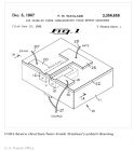
1959 年 “ 平面 ” 制造工艺的发明 Jean Hoerni 发展平面工艺解决了晶体管可靠性问题 , 从而使半导体制造革命化。 与台面晶体管( 1958 里程碑)的可靠性问题寻求解决方案, Fairchild 的物理学家 Jean Hoerni 回忆起他曾在 1957 年 12 月记录的想法 — 一个新的进程,在离开氧化层的硅片上,以保护敏感的 PN 下面的路口。由于专注于首批设备的投入生产,在那时该公司没有追求这种做法。 由于担心可能的污染物,传统的智慧,也需要去除氧化物掩蔽完成后这一层,从而暴露了路口。 Hoerni 观看氧化物,而不是作为一种可能的解决方案 - 他的“平面”的方法,成品设备的地势平坦而命名,会保护这些路口。在 1959 年 1 月编写了专利披露后,那年三月,他证明了工作平面晶体管的存在。就像霍尔尼曾预言过的,确实发现氧化层保护的路口。 平面器件也被证明有更好的电气特性 - 尤其是远低漏电流,这是计算机逻辑设计中的关键。他们允许从一个晶圆( 1960 里程碑)侧面制造集成电路的所有组件。 1960年4月,仙童公司推出了商业性的2N1613平面晶体管,并注册了该工艺在工艺中的所有权。今天的 10 亿个晶体管的集成电路全部依靠的是 Hoerni 的突破性理念。一位历史学家称它是“在半导体产业史上最重要的创新。” 虽然平面技术使硅晶体管以满足航空航天工业的严格要求,但是半导体厂商在遇到的每一个重大的技术进步的同时也会遇到新的麻烦。在 20 世纪 60 年代的重大问题,包括金丝上的“紫色的瘟疫”,铝与电的连线,和 MOS 晶体管的稳定。 1964 年(里程碑) 图一: 1 Jean Hoerni with transistor geometry in the background Jean Hoerni 在晶体管几何背景下的的照片 图二: Photomicrograph of a Model 2N1613 planar transistor 2N1613 平面晶体管模型的照片 图三: Figure from Hoerni’s patent on the planar manufacturing process Hoerni 的从图上显示的平面制造工艺过程的照片 图四: Cutaway view of an early Fairchild planar transistor 早期 Fairchild 平面晶体管的剖视图 译者:哈尔滨工业大学(威海)电子封装 090840124-于凯先 校对: 原文: http://www.computerhistory.org/semiconductor/timeline/1959-invention-of-the-planar-manufacturing-process-24.html 版权 copyright by www.computerhistory.org 原文: 1959 - Invention of the "Planar" Manufacturing Process Jean Hoerni develops the planar process to solve reliability problems of the mesa transistor, thereby revolutionizing semiconductor manufacturing. Seeking a solution to reliability issues with the mesa transistor ( 1958 Milestone ), Fairchild physicist Jean Hoerni recalled an idea he had recorded in December 1957 - a new process in which the oxide layer is left in place on the silicon wafer to protect the sensitive p-n junctions underneath. Focused on getting its first devices into production, the company did not pursue the approach at that time. Due to concerns about possible contaminants, conventional wisdom required removing this layer after completion of oxide masking, thus exposing the junctions. Hoerni viewed the oxide instead as a possible solution - his "planar" approach, named after the flat topography of the finished device, would protect these junctions. After writing a patent disclosure in January 1959, he demonstrated a working planar transistor that March. The oxide layer was indeed found to protect the junctions, as Hoerni had predicted. Planar devices also proved to have better electrical characteristics - particularly far lower leakage currents, which is critical in computer logic design. And they permitted fabrication of all the components of an integrated circuit from one side of a wafer ( 1960 Milestone ). Fairchild introduced the 2N1613 planar transistor commercially in April 1960 and licensed rights to the process across the industry. The billion-transistor integrated circuits of today rely on Hoerni’s breakthrough idea. One historian has called it "the most important innovation in the history of the semiconductor industry." While planar technology enabled silicon transistors to meet the stringent demands of the aerospace industry, semiconductor vendors continued to encounter new failure mechanisms with every major technology advance. Significant issues in the 1960s included “purple plague” on gold bonding wires, electromigration of aluminum interconnect lines, and MOS transistor stability. ( 1964 Milestone )
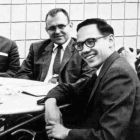
1960-第一个平面集成电路的制作 Jay Last引领了基于Hoerni的平面法和Noyce的整体方法的第一个商用IC的发展。 1959年8月Fairchild半导体研发主任Robert Noyce让共同创立者Jay Last开始开发一个基于Hoerni的平面法(1959里程碑)和Noyce的专利(1959里程碑)的平面集成电路。在Wescon用分立晶体管建立了一个多芯片触发器来诠释概念之后,Last组成了一个包括Sam Fok, Isy Haas, Lionel Kattner, 和 James Nall的团队。根据应用部门的Don Farina, Robert Norman提供的特性化数据,用一个改良的直接耦合晶体管逻辑(DCTL)电路设计了一个带有4晶体管和5个电阻器的兼有早期平面处理能力集成电路。 在一个芯片上集成多重相连的装置造成了许多新的工程挑战。1960年5月26日生产的第一个工作的单块集成电路设备使用了物理隔离来实现组件之间的电隔离。硅晶圆的背面刻蚀了深凹槽并且充满了不导电的环氧树脂。由Haas and Kattner研发的用硼扩散技术来实现p-n节电子隔离成为了首选的生产方法,并在1960年9月27日投入了集成电路的生产。 1960年Fairchild在工程会议提出了先进的信息并提供了面向的客户原型样品。在名为Logic (Micrologic)的贸易下,”F” 类型触发器功能在1961年通过一个在纽约的新闻发布会上展示广告和《生活》杂志上的一张照片向社会公告。五个包括" G "类型门功能(1962里程碑),半加法器和一个半移位寄存器的外加的电路在10月被应用。 Jay Last with Gordon Moore in background Jay Last和Gordon Moore在背景下 Credit: Fairchild Camera Instrument Corporation Physically-isolated Micrologic flip-flop compared to a dime from LIFE magazine March 10, 1961 物理隔离的微程序控制逻辑触发器与硬币相比,摘自1961年3月10日的生活杂志 Credit: Fritz Goro, Time Life Pictures Junction-isolated version of the type "F" flip-flop. The die were etched to fit into a round TO-18 transistor package 节孤立版本的“F”类型触发器。晶片被蚀刻来适应一个圆TO-18晶体管封装。 Credit: Fairchild Camera Instrument Corporation Presentation block with a Micrologic wafer and IC in the TO-18 package 一个微程序控制逻辑晶圆和集成电路在圆TO-18晶体管封装中的展示块 CHM collection: Gift of Bob and Marcella Major 译者:哈尔滨工业大学(威海)电子封装 090840126-种兆永 校对:哈尔滨工业大学(威海)电子封装 090840124-于凯先 原文 http://www.computerhistory.org/semiconductor/timeline/1960-FirstIC.html 版权 copyright by www.computerhistory.org ———————————————————————————————————— 1960 - First Planar Integrated Circuit is Fabricate Jay Last leads development of the first commercial IC based on Hoerni’s planar process and Noyce’s monolithic approach. In August 1959 Fairchild Semiconductor Director of RD, Robert Noyce asked co-founder Jay Last to begin development of an integrated circuit based on Hoerni’s planar process ( 1959 Milestone ) and Noyce’s patent. ( 1959 Milestone ) After building a multi-chip flip-flop with discrete transistors to demonstrate the concept at Wescon, Last assembled a team including Sam Fok, Isy Haas, Lionel Kattner, and James Nall. Based on characterization data prepared by Don Farina, Robert Norman of the applications department designed a flip-flop with four-transistors and five resistors using a modified Direct Coupled Transistor Logic (DCTL) circuit as most compatible with early planar processing capabilities. Integrating multiple interconnected devices on one chip posed many new engineering challenges. The first working monolithic devices produced on May 26 1960 used physical isolation to achieve electrical separation between components. Deep channels were etched from the rear of the silicon wafer and filled with non-conducting epoxy. The preferred production method, p-n junction electrical isolation using a boron diffusion technique developed by Haas and Kattner, yielded working circuits on September 27, 1960. Fairchild presented advanced information at engineering conferences and provided prototype samples to customers in 1960. Under the trade name Logic (Micrologic), the type "F" flip-flop function was announced to the public in March 1961 via a press conference at the IRE Show in New York and a photograph in LIFE magazine. Five additional circuits, including the type "G" gate function ( 1962 Milestone ), a half adder, and a half shift register, were introduced in October.
图1 Dawon Kahang的金属氧化物半导体(mos)晶体管的图形 M. M. (John) Atalla and Dawon Kahn g 在 1995 年于贝尔实验室成功制造了第一个绝缘栅极场效应晶体管,一直被 Lilienfeld, Heil, Shockley 等人长期期望的通过注入到半导体材料来克服表面态从而封锁电场。通过研究二氧化硅热生长层,他们发现这些 ** 会在一个由金属(金属极),氧化物(氧绝缘层),硅(硅半导体)组成的三明治(也就是 金属氧化物半导体场效应晶体管,通常被成为金属氧化物半导体 )的硅及其氧化物之间有一个明显的减小。因为他们的装置缓慢而起在电话系统中没有很急切的需求,所以它没有进一步的发展。在一个 1961 年的备忘中, Kahng 却指出了它在易于制造和在集成电路方面应用的可能性的潜力,飞兆半导体和美国无线电公司的研究人员认识到了这些优势。在 1960 年 Karl Zaininger 和 Charles Meuller 在美国无线电公司制造了一个 金属氧化物半导体晶体管,飞兆半导体的 C.T. Sah 制造了一个可控金属氧化物半导体四极管。 Fred Heiman and Steven Hofstein 随后在美国无线电公司于 1962 年研制出了 实验用 16 个晶体管的集成装置。 图2仙童半导体的FI 100 的p沟道金属氧化物半导体开关晶体管 金属氧化物半导体晶体管的导电区域要么是 p 型 ( 称其 p 沟道 设备 ) 或 n 型 (n- 沟道设备 ) 材料,后者要比 p 沟道的更快,同时也更难制作。 金属氧化物半导体器件 在 1964 年冲击了商业市场。通用微电子公司和飞兆半导体公司将 p 型装置用于逻辑开关。美国无线电公司引进了一种 n 沟道的晶体管用于放大信号。由于它比双极性器件有更小的尺寸和功率消耗,如今超过百分之 99 的微型芯片都用金属氧化物半导体器件来制作。取得这样的普遍应用耗费了十年努力。 图3 RCA16金属半导体晶体管的电路放大图像 图4 1962年在RCA的 MOS IC开发者 Steven Hofstein 译者:哈尔滨工业大学(威海)电子封装 090840127-周超 校对:哈尔滨工业大学(威海)电子封装 090840128- 徐涛 原文 http://www.computerhistory.org/semiconductor/timeline/1978-PAL.html 版权 copyright by www.computerhistory.org ———————————————————————————————— 1960 - Metal Oxide Semiconductor (MOS) Transistor Demonstrated John Atalla and Dawon Kahng fabricate working transistors and demonstrate the first successful MOS field-effect amplifier. In 1959 M. M. (John) Atalla and Dawon Kahng at Bell Labs achieved the first successful insulated-gate field-effect transistor (FET), which had been long anticipated by Lilienfeld, Heil, Shockley and others ( 1926 Milestone ) by overcoming the surface states that blocked electric fields from penetrating into the semiconductor material. Investigating thermally grown silicon-dioxide layers, they found these states could be markedly reduced at the interface between the silicon and its oxide in a sandwich comprising layers of metal (M - gate), oxide (O - insulation), and silicon (S – semiconductor) - thus the name MOSFET, popularly known as MOS. As their device was slow and addressed no pressing needs of the telephone system, it was not pursued further. In a 1961 memo, however, Kahng pointed out its potential ease of fabrication and the possibility of application in integrated circuits. But researchers at Fairchild and RCA did recognize these advantages. In 1960 Karl Zaininger and Charles Meuller fabricated an MOS transistor at RCA and C.T. Sah of Fairchild built an MOS-controlled tetrode. Fred Heiman and Steven Hofstein followed in 1962 with an experimental 16-transistor integrated device at RCA. The MOS transistor conducting region is either p -type (making it a p -channel device) or n -type ( n -channel device) material. The latter are faster than p -channel but are more difficult to make. MOS devices hit the commercial market in 1964. General Microelectronics (GME 1004) and Fairchild (FI 100) offered p -channel devices for logic and switching applications; RCA introduced an n -channel transistor (3N98) for amplifying signals. Because of their smaller size and lower power consumption than bipolar devices, over 99 percent of microchips produced today use MOS transistors. Achieving such ubiquity took decades of effort. ( 1964 Milestone )
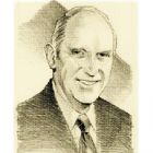
1960年外延沉积过程中提高晶体管的性能 薄膜晶体生长过程的发展,导致具有高转换速度的晶体管。 1951年,戈登舠尔和霍华德克里斯滕森在贝尔实验室开发的一个现在被称为外延沉积过程,此过程成长在基板上,继续底层基板上成长一层薄的材料晶体结构。 sheftal',Kokorish,和Krasilov在苏联1957年描述过硅和锗类似的工作过程。 在伊恩圠斯的敦促下,1960年由亨利瘠鶖尔领导的贝尔实验室团队用化学气相沉积增加基层和晶体管集电极之间的薄硅外延层。这种方法不仅提高了晶体管的击穿电压同时显著提高了开关速度(1961年的里程碑)这两个重要的电路设计特点。额外的工艺步骤添加的制造成本比被设备改善的性能还要多。这项技术很快的传到了西方电气公司,并在通过贝尔系统转换的电子电话硅晶体管的制造业中使用。 陶依尔的一个外延晶体管的介绍在1960年6月的固态设备研究会议引起了广泛的关注。 Fairchild公司用外延工艺制造的2N914,在1961年3月推出其最成功之一的晶体管,并迅速被Rheem, Sylvania和Texas仪器公司效仿。 摩托罗拉将此工艺应用在大规模生产汽车交流发电机设备过程中, 硅外延工艺在早期双极集成电路制造业产量的重要影响,使个别电路元件电气隔离的完成更加容易。后来广泛应用在MOS产品制造生产中。外延生长技术也常用在形成超薄层的复合半导体制造中。 图一 伊恩罗斯作为贝尔实验室的董事长的素描像 Pencil sketch of Ian Ross as president of Bell Labs 2006-2007 Alcatel-Lucent. All rights reserved 图2 单一外延工艺反应装置图 Diagram of a simple epitaxial reactor 2006-2007 Alcatel-Lucent. All rights reserved 图3 在运行当中的外延反应装置研究模型图 A research-scale epitaxial reactor in operation Credit: University of South Carolina 图4 外延晶体管在贝尔数字切换系统的应用图 Epitaxial transistors were used in the Bell Number One ESS switch Credit: ATT Corporate History 译者:哈尔滨工业大学(威海)电子封装 090840128-徐涛 校对:哈尔滨工业大学(威海)电子封装 090840127-周超 原文 http://www.computerhistory.org/semiconductor/timeline/1960-Epitaxial.html 版权 copyright by www.computerhistory.org 1960 - Epitaxial Deposition Process Enhances Transistor Performance Development of thin-film crystal-growth process leads to transistors with high switching speeds. In 1951 Gordon Teal and Howard Christensen at Bell Labs developed a process, now called epitaxial deposition, to grow a thin layer of material on a substrate that continues the underlying crystalline structure. Sheftal’, Kokorish, and Krasilov described similar work on germanium and silicon in the U.S.S.R. in 1957. At the urging of Ian Ross, a Bell Labs team led by Henry Theurer used chemical-vapor deposition to add a thin epitaxial layer of silicon between the base and collector of a transistor in 1960. This approach raised the transistor’s breakdown voltage while dramatically increasing its switching speed, (1961 Milestone) two important circuit-design characteristics. The added manufacturing cost of the extra process step was more than offset by improvements in device performance. The technology was quickly transferred to Western Electric and used in manufacturing silicon transistors for electronic telephone switching in the Bell System. Theurer gave a presentation on epitaxial transistors at the June 1960 Solid-State Device Research Conference that aroused widespread interest. Fairchild used epitaxy to fabricate the 2N914, one of its most successful transistors introduced in March 1961 and quickly emulated by Rheem, Sylvania, and Texas Instruments. Motorola applied the process to mass produce devices for automotive alternators. Epitaxial silicon also had an important impact on the manufacturing yield of early bipolar integrated circuits by allowing electrical isolation of the individual circuit components to be accomplished much more easily. It later found widespread application in the manufacture of MOS products. Epitaxial growth techniques are also used to form the ultra-thin layers common in compound-semiconductor manufacturing.
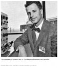
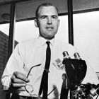
1961- 硅晶体管超过锗晶体管的速度 计算机工程师 西摩 · 克雷基金发展第一个硅装置来满足世界上最快机器的性能要求。 在通用自动电子计算机方面,计算机工程师西摩 · 克雷曾经致力于通用晶体管公司的锗晶体管。在和 威廉 · 诺里斯一成立数据控制公司,克雷就让通用晶体管公司为 CDDC 1604 计算机生产出了快速切换的锗设备,这个计算机在 1960 年成为了第一个商业成功的大型科学计算晶体管机器。 为了创造世界上最快的超级计算机,克雷要求一个在成百上千设备近距离工作产生的高温环境中运行且能在 3 纳秒之内切换的晶体管。 克雷授予飞兆半导体公司 500 , 000 美元的开发合同要为 CDC 6600 制造一个新的晶体管。 吉恩 · 赫尔尼达到了技术要求,结合 “ 掺金 ”—— 除了黄金杂质 - 连同新的外延沉积过程。该 2n709 ( ft-1310npn 型装置)在 1961 年 7 月作为第一类超越锗速度的硅晶体管被介绍推出。 每一个 CDC 6600 用 600 , 000 个晶体管封装在一个独特的 cordwood-style 模块配置中来减少连接电线的长度。在 1964 年飞兆半导体因为超过一千万的设备被成为“半导体产业历史上最大的单一指令之一”。科学数据系统是另一个在西格玛系列电脑逻辑应用中高速硅半导体的早期采纳者。 Jean Hoerni working in the lab 图片 1 :吉恩 · 赫尔尼正在实验室工作。 。 2N709 die - epitaxial gold-doped switching transistor 图片 2 : 2N709 晶圆外延开 掺金开关晶体管。 CDC 6600 "cordwood-module" transistor-based logic units 图片 3 : CDC 6600”cordwood 模块 ” 电晶体逻辑组合。 Open logic and memory "leaves" of a CDC 6600 图片 4 : CDC 6600 的开放式逻辑与记忆的“叶子”。 版权 copyright by www.nobeprize.org 译者:哈尔滨工业大学(威海)电子封装 090840129-祝乐 校对:哈尔滨工业大学(威海)电子封装 090840112-李迪 1961 - Silicon Transistor Exceeds Germanium Speed Computer architect Seymour Cray funds development of the first silicon device to meet the performance demands of the world’s fastest machine. Computer architect Seymour Cray had worked with General Transistor Corporation’s germanium transistors at Univac. On founding Control Data Corporation in 1957 with William Norris, Cray asked General Transistor to develop a fast switching germanium device for the CDC 1604 that in 1960 became the first commercially successful large-scale transistor machine for scientific computing. With the goal of building the world’s fastest supercomputer, Cray required a transistor that switched in less than 3 nanoseconds while operating in a high temperature environment created by hundreds of thousands of devices operating in close proximity. Early silicon transistors offered superior operation to germanium at elevated temperature but were too slow for many computer designs. Cray awarded Fairchild Semiconductor a $500,000 development contract to build a new transistor for the CDC 6600. Jean Hoerni met the specification by combining "gold-doping" - the addition of gold impurities - together with the new epitaxial deposition process. ( 1960 Milestone ) The 2N709 (FT-1310) n-p-n device was introduced in July 1961 as the first silicon transistor to exceed germanium speed. Each CDC 6600 used 600,000 transistors packaged in a unique cordwood-style module configuration to minimize connecting wire lengths. In 1964 the company placed "one of the largest single orders in the history of the semiconductor industry" with Fairchild for over 10 million devices. Scientific Data Systems was another early adopter of high-speed silicon transistors for logic applications in the Sigma series computers.
1962年-航天航空系统首先在计算机中应用集成电路 在军事和航空航天系统中,集成电路的尺寸,重量和降低功耗设计相比于分立式晶体管来说更证明了它高成本的合理性。 第一个集成电路仅仅取代了少数元件,速度相对迟缓,但卖价却是它相对应的分立式晶体管价格的好多倍。所以航空航天和军事系统是少数应用这种低功耗和小尺寸的应用程序的系统。 1961 年杰克基尔比的同事哈维克瑞根为美国空军演示“分子的电子化计算机” 来证明 587 个美国德州仪器集成电路在通用设计中可以代替 8500 个晶体管和其它组件来完成同样的功能。 自 1961 年,飞兆半导体微程序控制逻辑装置( 1960 年重要事件)被设计进交流火花塞和马丁马太克 420 计算机中,而不是在美国国家航空和宇宙航行局的阿波罗制导计算机(自动增益控制)中,成为最有意义的早期项目。此装置由麻省理工大学于 1962 年设计,并由雷声公司建成,每个系统大约使用了 4000 个 “G 类型 ” ( 3- 输入或非门)电路。到 1965 年,自动增益控制是集成电路最大的使用者,每个在 20 到 30 美元之间消耗 2000 个单位。 工程师库克设计 51 系列直接耦合晶体管逻辑电路,这是德州仪器的首次平面集成电路系列,以此来满足美国国家航空和宇宙航行局的行星间检测探针( IMP )的光纤层面计算机低功耗的标准。接口信息处理器卫星使用 510 款和 514 款作为二进制计数器,触发器和禁止电路,并于 1963 年携带首个集成电路绕轨道运行。在 1962 年德州仪器赢得一份与北美飞机制造业自动控制部门的合同,来为民兵二的导弹制导系统设计 22 习用电路。可莱维特和西屋电器也为民兵计划制造环路,并且在 1965 年取代了美国国家航空和宇宙航行局的阿波罗电子采购成为唯一一个集成电路的最大消费者。 费兰蒂股份有限公司研发的编码器。属于英国开发的微 NOR ,是欧洲最早的集成电路逻辑系列之一, 1961 年使英国皇家海军系统飞机上的计算机系统小型化。 Philco Ford also produced the Fairchild Type "G" Micrologic gate for the Apollo Guidance Computer Credit: Philco-Ford Microelectronics 飞哥福特还为阿波罗制导计算机生产了“ G ”类型微程序控制逻辑门飞兆半导体 资源出处:飞哥福特微电子科技 Apollo logic module assembled by Raytheon Credit: U. S. National Aeronautics and Space Administration 由雷声公司组装的阿波罗逻辑模块 资源出处:美国国家航空和宇宙航行局 Eldon C. Hall, MIT Instrumentation Laboratory lead hardware designer for the AGC promoted the use of integrated circuits Credit: MIT Archives 埃尔登 C ,麻省理工学院测试试验实验室为自动增益控制促进集成电路的使用主要计算机硬件设计者 资源出处:麻省理工学院档案 TI's "Molecular Electronic Computer" brochure prepared to accompany the demonstration machine on a tour of military contractors Courtesy of: Texas Instruments, Inc. 德州仪器准备在一次军事合约商洽谈中伴随机器示范的“分子化电子计算机”宣传册 提供途径:德州仪器公司 译者:哈尔滨工业大学(威海)电子封装 090840202-顾佳慧 校对:哈尔滨工业大学(威海)电子封装 090840203-李丹 原文 http://www.computerhistory.org/semiconductor/timeline/1962-Apollo.html 版权 copyright by www.computerhistory.org ——————————————————————————————————————————————————————— The size, weight, and reduced power consumption of integrated circuits compared to discrete transistor designs justify their higher cost in military and aerospace systems. The first integr ated circuits were relatively slow, replaced only a handful of components, and sold for many times the price of their discrete transistor counterparts. Aerospace and military systems were among the few applications where the low power consumption and small size outweighed these drawbacks. In 1961 Jack Kilby’s colleague Harvey Cragon built a demonstration "Molecular Electronic Computer" for the US Air Force to show that 587 TI ICs could replace 8,500 transistors and other components that performed the same function in a conventional design. Beginning in 1961, Fairchild Micrologic devices ( 1960 Milestone ) were designed into the AC Spark Plug MAGIC and Martin MARTAC 420computers but NASA's Apollo Guidance Computer (AGC) was the most significant early project. Designed by MIT in 1962 and built byRaytheon, each system used about 4,000 “Type-G” (3-input NOR gate) circuits. Consuming 200,000 units at $20-30 each, the AGC was the largest user of ICs through 1965. Engineer Bob Cook designed Series 51 DCTL, Texas Instruments' first planar IC family, to meet a low-power specification for the Optical Aspect Computer on NASA’s Interplanetary Monitoring Probe (IMP). Using the SN510 and SN514 as binary counters, flip-flops, and inhibiting circuits, the IMP satellite carried the first ICs into orbit in 1963. In 1962 TI won a contract from the Autonetics Division of North American Aviation to design 22 custom circuits for the Minuteman II missile guidance system. Clevite and Westinghouse also developed circuits for the Minuteman project, which by 1965 overtook NASA’s Apollo procurement as the largest single consumer of ICs. Ferranti Semiconductor Ltd. of England developed MicroNOR, one of Europe's first IC logic families, in 1961 to miniaturize on-board computing systems in UK Royal Navy systems.
1963年标准逻辑集成电路家族介绍 二极管 - 晶体管逻辑电路 (DTL) 家族为数字集成电路创造了广大的市场,但是到二十世纪六十年代末期在速度,成本及集成度方面占优势的改进型肖特基晶体管(TTL)成为了最流行的标准逻辑配置。 分离二极管 - 晶体管逻辑电路 (DTL) 的完整版本成为了第一个大量 IC 产品生产线。贝克·奥威尔在 1962 年设计的, se100 系列的 DTL 家族被 Fairchild 的 930 系列创造的一个有竞争力的跳背模式产品以其更小的噪音,更便宜的价格优势所赶超,这种产品一直沿用至今。 Pacific Semiconductor 的 James Buie 在 1961 年申请专利, TTL (晶体管—晶体管逻辑电路)作为以后二十年里最受欢迎的逻辑配置出现。没有注意到 Bule 的成果,但是因为 Ruegg 和 Fairchild 的 Beeson 描绘的“完全晶体管”逻辑电路模型而有了灵感, Thomas Longo 在 1963 年领导设计了第一个 TTL 家族——西尔维尼亚万能高电平逻辑电路( SUHL )。被 SUHL 在凤凰导弹应用的成功所激励, TI 在第二年生产了有竞争力的 TTL 家族的 SN5400 系列 。这个公司在 1966 年发布的 SN7400 系列是为工业顾客设计的低成本的塑料封装,它迅速占领了逻辑领域超过百分之五十的市场。 到 1968 年,平板印刷术很大的增加了整合在芯片上的晶体管的数量,热切地希望在 TTL 产业占一定的份额, Fairchild ( 9300 系列)和 Signetics ( 8200 系列)开拓了 TTL-MSI (中等规模集成—每个芯片上升至 100 个逻辑入口) 结的设计制造,比如计数器,注册转移和算术逻辑部件。一些卖家应用萧特基( 1969 年的里程碑)和互补型金属氧化物半导体( 1963 年的里程碑)技术去建立更大,更快,耗能更低的 TTL 兼容结,它拓宽了有效年限和这种受欢迎的逻辑配置的申请范围。 Introduced 2 years after Signetics SE124 DTL flip-flop, Fairchild's 930 series DTL (right) was smaller and therefore cheaper and faster Credit: Fairchild Camera Instrument Corporation Signetics的SE124DTL触发器引入两年后,Fairchild的930系列DTL更小因此成本更低更快 Dr. Thomas A. Longo developed SUHL TTL at Sylvania in 1963 Credit: Fairchild Camera Instrument Corporation Thomas A. Longo博士于1963年在西尔维尼亚研制了SUHL TTL The indispensable data manual of the 1970s Courtesy of: Texas Instruments, Inc 1970系列必不可少的的数据手册 Am9300 TTL MSI universal shift register. AMD’s first product was an improved version of the Fairchild original CHM Collection. Photo gift of Ed Turney Am9300 TTL MSI 的通用转换缓存器,AMD的第一个产品是一个Fairchild原始版本的改进版 译者:哈尔滨工业大学(威海) 电子封装 090840204-马聪 校对:哈尔滨工业大学(威海)电子封装 090840206-杨英坤 原文: http://www.computerhistory.org/semiconductor/timeline/1963-TTL.html 版权 copyright by www.computerhistory.org 1963 - Standard Logic IC Families introduced Diode Transistor Logic (DTL) families create a high-volume market for digital ICs but speed, cost, and density advantages establish Transistor Transistor Logic (TTL) as the most popular standard logic configuration by the late 1960s. Integrated versions of discrete diode transistor logic (DTL) circuits became the first high-volume IC product lines. Designed by Orville Baker in 1962, the Signetics SE100 Series DTL family was overtaken in 1964 by the better noise immunity and lower cost of Fairchild's 930 Series establishing a competitive industry leap-frog pattern that continues today. Patented by James Buie of Pacific Semiconductor in 1961, TTL (Transistor Transistor Logic) emerged as the most popular logic configuration of the next two decades. Unaware of Buie's work but inspired by an "all transistor" logic circuit described by Ruegg and Beeson of Fairchild, Thomas Longo led the design of the first TTL family, Sylvania Universal High-level Logic (SUHL) in 1963. Encouraged by SUHL's success in winning a high-profile Hughes military design (the Phoenix missile), TI introduced the competing SN5400 Series TTL family the following year. The company announced the SN7400 Series in low cost plastic packages for industrial customers in 1966 and quickly gained a greater than 50% share of the logic market. By 1968 lithography advances significantly increased the number of transistors that could be integrated on a chip. Eager to win a share of the TTL business, Fairchild (9300 Series) and Signetics (8200 Series) pioneered the design of TTL-MSI (Medium Scale Integration - up to 100 logic gates per chip) functions such as counters, shift registers, and arithmetic logic units. Many vendors applied Schottky ( 1969 Milestone ) and CMOS ( 1963 Milestone ) technology to build larger, faster, and lower power TTL-compatible functions that extended the useful life and range of applications of this popular logic configuration.
半导体里程 _ 博物馆 _ 第一个商业MOS集成电路的介绍 Andy Grove, Bruce Deal, and Ed Snow discuss MOS technology at the Fairchild Palo Alto R D laboratory in 1966 Credit: Fairchild Camera Instrument Corporation 图一 安迪 · 格鲁夫 , 布鲁斯 · 帝尔 , 艾德 · 雪飞在帕洛阿尔托的飞兆半导体研发实验室探讨 MOS 技术于 1966 年 一般微电子使用一种金属氧化物半导体 (MOS) 处理来在芯片上装比双极集成电路更多的晶体管,并使用这项技术建立了第一个计算器芯片组。 由于复杂的制造和可靠性问题,所以实现 MOS 关于比双级( 1960 里程碑)高密度和低成本的承诺比预期的更困难。在研讨会上的发言者把在电子学方面的失败的物理现象与盲人摸象的故事做比较 -— 这主要取决于你检查哪一部分。 1961 年弗雷德里克· 海曼 和史蒂文·奥弗斯坦在美国无线电公司做了个关于 16 晶体管集成电路的实验并且后来在了解表面氧化物质量方面做出了重要贡献。在 1963 年和 1966 年之间,布鲁斯·帝尔,安德鲁·格鲁夫和艾德·雪尔在仙童 半导体公司 鉴定了纳污染问题并且出版了很多关于氧化物的电性性质的论文这些为格鲁夫的经典教材《物理和半导体设备技术》提供了资料。世界各地的合作与竞争,包括来自 NEC · IBM ·飞利浦的研究者在最后的十年中解决了基本的产量和可靠性问题使得 MOS 作为主导的 IC 技术出现。 R. P. Donovan’s illustration of the spectrum of MOS instability explanations presented at a 1966 symposium Courtesy of: Bruce Deal and Harry Sello 图二 R.P 多诺万的关于 MOS 不稳定性的图解在 1966 年的一个研讨会上呈现 The first commercial MOS IC, GMe's 20-bit shift register used 120 p-channel transistors in 1964 CHM Collection. Photo gift of Don Farin 图三 第一个用了 120 个通道的 晶体管的商用 MOS IC 、 GMe 的 20-bit 移位寄存器在 1964 年 1964 年当罗伯特·诺曼使用一个二阶段时钟计划来设计一个用 120p 通道晶体管的 20 位移位寄存器时,普通的微电子推出了第一个商业 MOS 集成电路。 1965 年, GMe 作为第一个基于 MOS 的电子计算操纵者为 维克特康普托计算机 设计了 23 位自定义集成电路。 飞哥福特 收购了该公司并且将业务转移到费城大多数员工转移到其他公司后,在 航空英里指示器 及通用仪器方面继续蓬勃发展计算机芯片市场。 The prototype Victor Comptometer EC-3900 calculator and board with 23 custom MOS chips and six 100-bit shift registers for serial memory CHM Collection. Gift of Don Farina 图四康普托计算机原型 EC- 3900 计算器和在 23 个自定义 MOS 芯片和六个 100 位移位寄存器和串行存储器 到 1969 年罗克韦尔微电子学为夏普的第一台便捷携带式机 microCompet QT-8D 已经将电子芯片数降到四台设备,并且继续前进成为上世纪 70 年代早期的计算机芯片最大供应商。 1971 年 泰克 及 美国德州仪器公司(1974 里程碑 ) 介绍了单片机 ( 除了外部显示器 ) 驱动程序解决方案 。 译者:哈尔滨工业大学(威海)电子封装 090840206- 杨英坤 校对:哈尔滨工业大学(威海)电子封装 090840204 马聪 原文 http://www.computerhistory.org/semiconductor/timeline/1964-Commecial.html 版权 copyright by www.computerhistory.org ——————————————————————— 1964 - First Commercial MOS IC Introduced General Microelectronics uses a Metal-Oxide-Semiconductor (MOS) process to pack more transistors on a chip than bipolar ICs and builds the first calculator chip set using the technology Achieving the MOS promise of higher density and lower cost than bipolar ( 1960 Milestone ) proved more difficult than anticipated due to complex manufacturing and reliability issues. Speakers at a symposium on the Physics of Failure in Electronics likened competing solutions to the story of the blind man and the elephant – it depends on which part you examine. Frederic Heiman and Steven Hofstein built an experimental 16-transistor IC at RCA in 1961 and later made important contributions to understanding surface oxide quality. Between 1963 and 1966, Bruce Deal, Andrew Grove, and Ed Snow at Fairchild identified the issue of sodium contamination and published many papers on the electrical nature of oxides that informed Grove’s classic textbook Physics and Technology of Semiconductor Devices. Collaboration and competition across the globe, including researchers from NEC, IBM and Philips, resolved the fundamental yield and reliability issues by the end of the decade that allowed MOS to emerge as the dominant IC technology. General Microelectronics introduced the first commercial MOS integrated circuit in 1964 when Robert Norman used a 2-phase clock scheme to design a 20-bit shift register using 120 p-channel transistors. GMe designed 23 custom ICs for the first MOS-based electronic calculator for Victor Comptometer in 1965. After the company was purchased by Philco-Ford and the operation transferred to Philadelphia most employees moved on to other companies, including AMI and General Instrument, where they continued to develop chips for a burgeoning calculator market. By 1969 Rockwell Microelectronics had reduced the chip count to four devices for Sharp's first portable machine, the microCompet QT-8D , and went on to become the largest supplier of calculator chips in the early 1970s. Mostek and TI ( 1974 Milestone ) introduced single-chip (except for external display drivers) solutions in 1971.
1964 年 - 第一个被广泛使用的模拟集成电路出现 大卫塔尔伯特和罗伯特维德勒在飞兆半导体通过建立商业上成功的模拟应用集成电路,开启了一个主要行业部门。 模拟,也称为线性电路,像声音,温度和无线电波那样电路放大和状态信号不断变化的现象。由于处理这些信号需要极高的分辨率,模拟电路要求在设计和制造中有很高的精度。模拟电子管运放的设计是由哥伦比亚大学的研究员露比朱莉的想法一步一步开发的。第一个锗晶体管运放出现在 1958 年,硅晶体管出现在 1960 年。在布尔布朗和菲尔布里克的研究之后不久 nexus 研究室于 1962 年推出第一个预配置的运放模块 。 艾米克,飞兆半导体,莲花,德州仪器和西屋电气公司开发了早期的模拟集成电路。西屋电气公司的林慧聪 1963 年在 Autonetics 民兵 2 导弹的传统运放上使用了片状元件匹配和外侧三极管专利。但是 1964 年由飞兆半导体公司的工艺工程师戴维卡尔伯特和设计师罗伯特韦德的团队发明的 μA702 运放才是第一个被广泛使用的商业产品。 1965 年的继承者 μA709 运放为模拟集成电路建立了巨大的市场。塔尔伯特和韦德在 1965 年末搬到 molectro (后来被国家收购),在那他们通过 lm101 开始建立了一个长久的王朝。然后在 1968 年飞兆半导体的戴维富嘉通过增加一个固有补偿电容第一次升级了 lm101 ,得到 μA741 ,这是有史以来最流行运放。 专业模拟集成电厂商为放大器,比较器,数据转换器,电源管理器件,和汽车,消费,通信应用周边的大量特点发展了广泛的产品目录。模拟器件通常比数字集成电路具有更长的寿命周期。例如有四十年历史的富嘉的 μA741 运放,汉斯 Camenzind Signetics 公司制造的 555 定时器在今天仍被广泛应用。 Robert Widlar inspects the LM10 mask layout circa 1977 Credit: National Semiconductor 罗伯特 · 维德拉 1977 年检查 LM10 版图 An early analog IC, the Fairchild μA700 differential amplifier designed by Bohumil Polata (1963) Credit: Fairchild Camera Instrument Corporation 早期的模拟集成电路,飞兆半导体的 μA700 : Bohumil Polata ( 1963 )设计的差分放大器 Talbert and Widlar's μA709 high-performance operational amplifier (1965) Credit: Fairchild Camera Instrument Corporation 塔尔伯特和维德拉的 μA709 高性能运算放大器( 1965 ) Widlar's LM10 op amp broke new ground for low voltage operation Credit: National Semiconductor 维德拉的 LM10 运算放大器打破了低电压差工作的新局面 译者:哈尔滨工业大学(威海)电子封装 090840207-邹运 校对:哈尔滨工业大学(威海) 原文 http://www.computerhistory.org/semiconductor/timeline/1964-analog.html 版权 copyright by www.computerhistory.org —————————————————————————————————————————————————— 1964 - The First Widely-Used Analog Integrated Circuit is Introduced David Talbert and Robert Widlar at Fairchild kick-start a major industry sector by creating commercially successful ICs for analog applications. Analog, also called linear, circuits amplify and condition signals from continually varying phenomena such as sound, temperature, and radio waves. Because of the nearly infinite resolution required to process these signals, analog circuits demand high precision in design and manufacturing. Analog vacuum tube operational amplifier (op-amp) designs were paced by the concepts developed by Columbia University researcher Loebe Julie. The first germanium transistor op-amp appeared in 1958 with silicon versions in 1960. Nexus Research Labs offered the first pre-configured op-amp modules in 1962 followed shortly by Burr-Brown and Philbrick Researches. Amelco, Fairchild, RCA, TI, and Westinghouse developed early analog ICs. H. C. Lin of Westinghouse employed on-chip component matching and his lateral PNP patent on a custom op amp for the Autonetics Minuteman II missile in 1963. But the Fairchild μA702 op amp, created in 1964 by the team of process engineer Dave Talbert and designer Robert Widlar, was the first widely-used commercial product. Their 1965 successor, the μA709, established a mass market for analog ICs. Talbert and Widlar moved to Molectro (later acquired by National) in late 1965 where they built a linear dynasty beginning with the LM101. Then in 1968 Dave Fullagar of Fairchild one-upped the LM101 by adding an internal compensating capacitor to deliver the μA741, the most popular op-amp of all time. Specialty analog IC manufacturers evolved extensive catalogs of amplifiers, comparators, data converters, power management devices, and numerous specialty circuits for automotive, consumer and communications applications. Analog devices typically have much longer life cyles than digital I/Cs. Examples of 40 year-old designs that remain widely used today include Fullagar's μA741 op-amp and the 555 timer created by Hans Camenzind for Signetics.
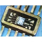
1965“摩尔定律”预测 集成电路的发展走向 戈登·摩尔,飞兆半导体公司的研发总监,在一篇内部文献中作了一张图,图中有一条通过五个点的线,代表着1959年至1964年间每片集成电路中一个元器件所需成本的变化情况。摩尔在《集成电子学的未来》这一文献中试图预测未来十年里集成电子学最可能的发展情况。当摩尔以每12个月器件数量翻一番的发展趋势在投影图上进行推断,他发现1975年每个芯片上的器件数目会达到65000个。《让集成电路填满更多元件》作为一篇杂志文章,于1965年4月19日发表在《电子》杂志上。 Gordon Moore at Fairchild R D in 1962 1962年戈登·摩尔在飞兆半导体公司研发中心 Credit: Fairchild Camera Instrument Corporation 在1975年的国际电子器件会议中,摩尔指出光刻方法,晶圆尺寸,工艺技术的发展,以及设备与装置的智能化,尤其是半导体存储器阵列化,能使他发现的规律得意现实。根据更多的近期数据,其中包括更高复杂程度(仅仅比存储器密度低)的微处理器设计,摩尔把未来器件复杂度的增加速率从一年翻一番降为两年翻一番。 Cost vs. time sketch from Moore's 1964 notebook 1964年,戈登·摩尔笔记本中成本与时间关系的草图 Credit: Fairchild Camera Instrument Corporation 这个预测成为一个自我实现的预言,成为半导体工业遵守的一个法则。专家指出年度突破挑战,以确保符合由卡弗·米德命名的“摩尔定律”。1995年,再次回顾产业现状时 (此时英特尔奔腾处理器含有近500万晶体管),摩尔说,“当前的预测是,这样的发展不会马上停止。”一个装置(美国)含有超过十亿个晶体管。 Dr. Moore revisits his projection with additional data gathered through 1975 摩尔博士获取1965年至1975年的新数据之后重新制作的投影图 Courtesy of: Intel Corporation Several of the chips in this photo provided data points for the 1965 article 图中的芯片为1965年发表的那篇文献提供了数据 Credit: Fairchild Camera Instrument Corporation 译者:哈尔滨工业大学(威海)电子封装 090840208-汪洋 校对:哈尔滨工业大学(威海)电子封装 090840209-常青 原文 http://www.computerhistory.org/semiconductor/timeline/1965-Moore.html 版权 copyright by www.computerhistory.org —————————————————————————————————————————————————————— 1965 - "Moore's Law" Predicts the Future of Integrated Circuits Fairchild’s Director of R D predicts the rate of increase of transistor density on an integrated circuit and establishes a yardstick for technology progress. Gordon Moore, Fairchild Semiconductor’s Director of RD, wrote an internal paper in which he drew a line through five points representing the number of components per integrated circuit for minimum cost per component developed between 1959 and 1964. "The Future of Integrated Electronics" attempted to predict "the development of integrated electronics for perhaps the next ten years." Extrapolating the trend to 1975 he projected that the number of components per chip would reach 65,000; a doubling every 12 months. Edited for publication as a magazine article, "Cramming more components onto integrated circuits" was published in Electronics on April 19, 1965. At the 1975 IEEE International Electron Devices Meeting Moore, by now with Intel, noted that advances in photolithography, wafer size, process technology, and "circuit and device cleverness," especially in semiconductor memory arrays, had allowed his projection to be realized. Adding more recent data, that included a higher mix of microprocessor designs that were somewhat less dense than memories, he slowed the future rate of increase in complexity to "a doubling every two years, rather than every year." This prediction became a self-fulfilling prophecy that emerged as one of the driving principles of the semiconductor industry. Technologists were challenged with delivering annual breakthroughs that ensured compliance with "Moore’s Law," as it was dubbed by Carver Mead. On reviewing the status of the industry again in 1995 (at which time an Intel Pentium microprocessor held nearly 5 million transistors) Moore concluded that “The current prediction is that this is not going to stop soon.” Devices exceeding one (U.S.) billion transistors exist today.
1965 主机开始采用集成电路 大型电脑制造商发布了基于定制和特殊用途的集成电路机器。 用于商业和科学计算的大型电子数据处理系统称为“主机”电脑。在十九世纪六十年代,主机供应商通过专有的硬件、操作系统和应用软件在市场上区分他们的系统。他们要求组件能提供不同的特性和比目前可用的通用逻辑系列更快的速度( 1961 年里程碑)。( 1963 年里程碑)由于这些系统提供了大量的商机,飞兆、摩托罗拉、 Signetics 公司、德州仪器及其他手工制作系列的工程师团队都申请定制特殊用途的集成电路。 最早一批设计使用单片集成电路的主机有 1966 年发布的巴勒斯 B2500/3500 、 RCA 光谱 70 系列( 1965 )和科学数据系统西格玛 7 ( 1966 )。巴勒斯的工程师和飞兆的 Robert Seeds 创建了互补晶体管逻辑体系并为惠普的 3000 系列创造了条件。 RCA 创建了电流型逻辑内部电路并与集成电路供应商合作生产它们。 SDS 和 Signetics 及另外几家公司合作完成一个六个设备的系列。 CDC 、通用电气、霍尼韦尔、 IBM 、 NCR 、 SDS 和 UNIVAC 等公司都创建了定制电路系列。 1962 年 1 月, Narud 领头创建了摩托罗拉的 MECL ( Motorola Emitter Coupled Logic 摩托罗拉发射极耦合逻辑)系列,一种单片实施了 IBM 公司基于晶体管的高速逻辑电路。虽然作为标准产品,昂贵的多层印制电路板和系统对冷却的要求限制了数据控制公司、 Cray 公司、通用电气、日立、 ICL 及其他公司对大量电子元件在科学计算机上的使用要求。 1976 年,每个克雷一号机器消耗 25 万对飞兆公司提供的 F100K 元件开关包,每个开关的转换时间都在 1ns 以内。 Describes how to specify a custom IC from Fairchild 图一 介绍如何从飞兆半导体公司定制指定的集成电路 Credit: Fairchild Camera Instrument Corporation A custom TTL gate design from 1964 图二 1964年设计的自定义TTL门电路 Credit: Fairchild Camera Instrument Corporation Burroughs B25/3500 Series used CTL ICs from Fairchild ITT 图三 飞兆半导体和ITT生产的巴勒斯B25/3500系列CTL集成电路 Credit: Burroughs Corporation RCA Custom CML circuits for the Spectra 70 computer 图四 RCA公司为光谱70计算机制造的CML集成电路 Credit: RCA Incorporated 译者:哈尔滨工业大学(威海)电子封装 090840209-常青 校对:哈尔滨工业大学(威海)电子封装 090840208-汪洋 原文 http://www.computerhistory.org/semiconductor/timeline/1965-Custom.html 版权 copyright by www.computerhistory.org ———————————————————————————————— 1965 - Mainframe Computers Employ ICs Large computer manufacturers announce machines based on custom and special purpose integrated circuits. Large electronic data processing systems for business and scientific applications are called "mainframe" computers. In the 1960s mainframe vendors distinguished their systems in the marketplace through proprietary hardware, operating systems, and applications software. They demanded components offering unique features and significantly faster speed (1961 Milestone) than the currently available general-purpose logic families. (1963 Milestone) As these systems offered high-volume production business opportunities, teams of engineers at Fairchild, Motorola, Signetics, TI, and others handcrafted families of custom and special purpose ICs for these applications. Some of the earliest mainframe designs to use monolithic ICs were the Burroughs B2500/3500 announced in 1966, RCA Spectra 70 series (1965), and Scientific Data Systems Sigma 7 (1966). Burroughs engineers cooperated with Robert Seeds at Fairchild to develop a Complementary Transistor Logic (CTL) family that also powered Hewlett-Packard’s 3000 Series. RCA developed Current Mode Logic (CML) circuits internally and worked with IC vendors to manufacture them. SDS worked with Signetics and others on a family of six devices. CDC, General Electric, Honeywell, IBM, NCR, SDS,and Univac also developed custom circuit families. In 1962 Jan Narud led the development of Motorola's MECL (Motorola Emitter Coupled Logic) family, a monolithic implementation of IBM's transistor-based very high speed logic circuits. Although offered as standard products, expensive multi-layer p.c. boards and system cooling requirements limited ECL usage largely to high-performance scientific computer applications at Control Data Corporation , Cray, GE, Hitachi, ICL, and others. In 1976 each Cray 1 machine consumed 250,000 dual F100K ECL gate packages from Fairchild that offered switching times of under 1ns per gate. n
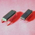
1965- 封装成为系统设计首要问题 摘要: 双列直插的封装格式显著简化 PCB 板布局并降低计算机的组装成本 大多数半导体器件采用陶瓷,金属或塑料等封装形式密封以防止芯片和脆性连接线的损坏。封装工艺尽管具有这样重要的功能,在半导体设计中却是最被疏忽的方面,芯片尺寸过大和功耗过多一直阻碍着封装进程发展。典型的 60 年代的三极管都采用的是带有 3 条外引线的 TO-5 或者 TO-18 金属罐封装。低成本的塑料形式主要用于气密性要求不高的产品,飞兆半导体第一次在最多容纳 10 条外引线的晶体管罐子上安装了微逻辑集成电路。为使航空电子设备上的芯片占有面积最小化,德州仪器的陶荣开发了一种 10 引线 0.25 , ,0125 英寸的扁平封装形式。 · 这些封装迭代大多数源自于现有格式,并不适用于高密度电路板的设计。 1965 年,飞兆半导体的 Don Forbes, Rex Rice, and Bryant ("Buck") Rogers 等人设计了一种 14 引线的,两侧带有 100 密尔的引脚的双列直插式封装形式,这样设计既简化了电路板的布局,又使得器件可自动插入 PCB 板,因此造就了一次计算机制造业的革命。 70 年代前期,低成本,塑料成型版的双列直插封装产量主导了整个产业,并且引脚数一直增加到 64 · 虽然大多数的 DIP 设计采用热压或超声波焊接到纯金或铝导线的芯片,一些厂商尝试用马丁 · 贝尔实验室 Lepselter 发明的微小的焊料凸点互连和改变光束引脚链接的方法,用于高可靠性的应用 前后修边的玻璃密封陶瓷双列直插封装 塑料DIP半剖示意图 摩托罗拉和德州仪器在DEC AXC板上安装的20引脚封装芯片 AMD公司在80年代中期的不同外形的DIP封装 译者:哈尔滨工业大学(威海)电子封装 090840210 高阳 校对:哈尔滨工业大学(威海) 原文 http://www.computerhistory.org/semiconductor/timeline/1978-PAL.html 版权 copyright by www.computerhistory.org 1965 - Package is the First to Accommodate System Design Considerations The Dual In-line Package (DIP) format significantly eases printed circuit board layout and reduces computer assembly cost. · Most semiconductor devices are enclosed in ceramic, metal or plastic packages to prevent damage to the chip and its fragile connecting wires. Despite this important function, packaging was one of the most neglected aspects of semiconductor design. Programs were delayed because the chip was too large or consumed too much power for the designated package. Typical 1960s transistors used TO-5 or TO-18 (Transistor Outline) metal-can packages with three external leads. Lower-cost plastic versions served applications not requiring a hermetic seal . Fairchild mounted its first Micrologic ICs in such transistor cans modified to accommodate up to 10-leads. Yung Tao at Texas Instruments developed a 10-lead, 0.25 by 0.125 inch flat-pack to occupy the smallest possible board area in avionics systems. · Most of these package iterations were derived from existing formats that were not conceived for high-density board designs. In 1965 Don Forbes, Rex Rice, and Bryant ("Buck") Rogers at Fairchild devised a 14-lead ceramic Dual-in-Line Package (DIP) with two rows of pins 100 mils apart that revolutionized computer manufacturing by simplifying layout and allowing automated insertion into printed circuit boards. Low-cost, plastic-molded versions of the DIP outline dominated production volumes by the early 1970s and pin-counts increased up to 64 leads. · While most DIP designs used thermo-compression or ultrasonic bonding to attach fine gold or aluminum wires to the chip, some vendors experimented with tiny solder bump interconnects and variations on a beam-lead approach invented by Martin Lepselter of Bell Labs for high-reliability applications.
1965-4-----半导体只读存储器芯片的出现 半导体只读存储器(光盘)提供高密度和低成本的单位比特 作为在制造过程中被写入只读存储器的永久数据,使用光盘存储的信息,在整个系统的生命历程中,将保持不变,如微程序代码,查找表,字符代码等。集成电路光盘由放置在行和列组织的信号线之间的二极管阵列组建成。晶圆制造过程中的最后一步是把以实现客户的代码所需的具体二极管连接起来。作为一个最小的存储单元结构的二极管, ROM 器件提供毎比特最高的密度和最低成本的半导体存储器。 在 1965 年,西尔韦尼亚为霍尼韦尔生产了一个 256 位的双极 TTL 电光盘,它由工厂里熟练的技术人员在一段时间内编写的,该人员从事把物理划片的金属环连接到选定的二极管的工作。定制面罩编程设备的生产订单是令人满意的。在 1965 年总微电子还开发速度较慢,但 四倍 1024 位光碟使用 MOS 技术。在 20 世纪 70 年代初,仙童,英特尔,摩托罗拉, Signetics 公司和 TI 提供 1024 位 TTL 光盘,而 AMD 公司, AMI ,电子阵列,通用仪器,国家,罗克韦尔和其他一些公司提供 4096 位( 4K ) MOS 器件。 首次大批量应用的桌面计算器消费被来自美国和日本厂商的设备其采用亿万 16K 和更大的器件视频游戏墨盒所超越。任天堂的超级马里奥兄弟 NES 游戏单独的生产超过 4000 万单位。由于每个 ROM 有顺序的被供应,客户经常为较长的交货时间和供应商的供货不及时而感到沮丧,以用户可编程的光盘( PROM 的)的形式来缓解。 Credit: Fairchild Camera Instrument Corporation 256-bit ROM number generator programming table 256位ROM数发生器编程表 Courtesy of: Intel Corporation Intel 3301, 1024-bit Bipolar ROM 英特尔3301 , 1024位双极光盘 CHM Collection. Electronic image gift of William Blair Electronic Arrays 8316F 16K MOS ROM with package lid removed 电子阵列8316F 16K MOS去掉包盖的 ROM CHM Dan Rose Packaging Collection. Gift of SEMI Atari video game cartridge board with AMD 4K-bit MOS ROM circa 1982 雅达利游戏机墨盒板与AMD的4K位MOS ROM大约在1982年 译者:哈尔滨工业大学(威海)电子封装 090840211-杜伟 校对:哈尔滨工业大学(威海) 高阳 原文 http://www.computerhistory.org/semiconductor/timeline/1965-ROM.html 版权 copyright by www.nobeprize.org 英文原文 1965 - Semiconductor Read-Only-Memory Chips Appear Semiconductor read-only-memories (ROMs) offer high density and low cost per bit. As data is permanently written into a Read Only Memory during the manufacturing process, ROM storage is used for information that will remain unchanged throughout the life of a system, such as microprogram code, look-up tables, character generation, etc. Integrated circuit ROMs are built from arrays of diodes placed between signal wires organized in rows and columns. The last masking step of the wafer fabrication process makes connection to the specific diodes required to implement the customer's code. As a diode represents the smallest possible memory cell structure, ROM devices offer the highest density and lowest cost per bit form of semiconductor memory. In 1965 Sylvania produced a 256-bit bipolar TTL ROM for Honeywell that was programmed one bit at a time by a skilled technician at the factory who physically scratched metal link connections to selected diodes. Production orders were satisfied with custom-mask programmed devices. Also in 1965 General Microelectronics developed slower but four-times larger 1024-bit ROMs using MOS technology. By the early 1970s Fairchild, Intel, Motorola, Signetics, and TI offered 1024-bit TTL ROMs, while AMD, AMI, Electronic Arrays, General Instrument, National, Rockwell and others produced 4096-bit (4K) MOS devices. Desktop calculator consumption, the first high-volume application, was surpassed by video game cartridges that used hundreds of millions of 16K and larger devices from U. S. and Japanese vendors. Production of Nintendo’s first Super Mario Brothers NES game alone exceeded 40M units. As each ROM is manufactured to order, customers were often frustrated with long delivery times and vendors overwhelmed by production logistics. Relief came in the form of user-programmable ROMs (PROMs). ( 1971 Milestone )
 标签: 半导体