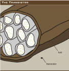
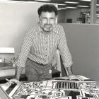
在一个电脑芯片上存在将近一百万的晶体管。甚至于在一些顶级的芯片上会呈现数亿的晶体管。为了能够让更多的晶体管可以很合适的装在和电脑芯片一样大小的东西上,这些晶体管需要十分小才可以满足要求。事实上,今天的晶体管已经发展到可以比人类的一根头发还要小很多倍的地步了。 译者:哈尔滨工业大学(威海)电子封装090330112-张慧颖 校对:哈尔滨工业大学(威海)电子封装090840205-钱政英 原文 http://www.nobelprize.org/educational/physics/transistor/function/small.html 版权 copyright by www.nobeprize.org Inacomputerchiptherecanexitasmanyasamilliontransistors.Insomeofthemostadvancedchipsevenseveralhundredsofmillionsoftransistorsarepresent.Tobeabletofitthatmanytransistorsintosomethingassmallasacomputerchip,theyneedtobeextremelysmall.Infacttoday'stransistorsaremany,manytimessmallerthanevenasinglehumanhair. Copyright copy; Nobel Media AB 2012 晶体管与一根头发的大小比较图
1874 年 半导体点接触整流效应的发现 在半导体二极管的第一份书面说明中,费迪南德·布劳恩指出,电流只在金属与方铅矿接触的那个接触点上自由地流动。 Ferdinand Braun 与 Guglielmo Marconi 共同获得 1909 诺贝尔物理学奖 费迪南德布劳恩在大学在法国斯特拉斯堡担任物理学教授 德国物理学家费迪南德 · 布劳恩 ,柏林大学24岁毕业生,于1874年在 Würzburg 大学研究 了电解质和晶体的导电特点。 当他探索一条晶体(铅硫化 物)方铅矿与点薄的金属丝时,布劳恩指出,电流只在一个方向流动。他发现了在金属与某些晶体材料接触点处的整流效应。 布 劳恩于1876年11月14日在莱比锡向听众 展示这样的半导体器 件,但它并没有发现任何有用的应用,直到无线电的出现,1900年代初期,它也被用于信号探测器在 “ 水晶电台 “ 设置。(1901里程碑) 常见的描述性名称 “ 猫的胡须 ” 探测器来源于用于制造电晶体表面接触的金属微细探针。布劳恩更为人所知的是在1897年发展阴极射线管(CRT)示波器,在德国被称为"百灵管 ” (Braunsche Rohre)。 他与古格列尔莫 · 马可尼共同获得1909年诺贝尔奖,因他们对 “ 无线电报的发展贡献”,主要开发可调谐回路为无线电接收机。 执行整流的电子设备被称为二极管。 1883 年,工作在爱迪生实验室的 William J. Hammer 在给加热丝灯泡补充另一个电极时发现了这种整流效应。 1904年,约翰·弗莱明发明了专利单程 ” 振荡阀",基于所谓的 “ 爱迪生效应 ” ,将交变电流无线电信号转换成耳机或扩音器中的直流电。 今日的二极管,也就是弗莱明阀门,是第一个实用的电子装置。布劳恩的点接触整流二极管执行同样的功能,是使用半导体特性而非热电子特性。 ——————————————————————————————— 译者:哈尔滨工业大学(威海)电子封装 090840102 冯怡 校对:哈尔滨工业大学(威海) 1874 - Semiconductor Point-Contact Rectifier Effect is Discovered In the first written description of a semiconductor diode, Ferdinand Braun notes that current flows freely in only one direction at the contact between a metal point and a galena crystal. Ferdinand Braun shared the 1909 Nobel Prize in Physics with Guglielmo Marconi Credit: www.cathodique.net Ferdinand Braun as a professor of physics at the University of Strasbourg in France Credit: www.cathodique.net German physicist Ferdinand Braun, a 24-year old graduate of the University of Berlin, studied the characteristics of electrolytes and crystals that conduct electricity at Würzburg University in 1874. When he probed a galena crystal (lead sulfide) with the point of a thin metal wire, Braun noted that current flowed freely in one direction only. He had discovered the rectification effect at the point of contact between metals and certain crystal materials. Braun demonstrated this semiconductor device to an audience at Leipzig on November 14, 1876, but it found no useful application until the advent of radio in the early 1900s when it was used as the signal detector in a "crystal radio" set. ( 1901 Milestone ) The common descriptive name "cat’s-whisker" detector is derived from the fine metallic probe used to make electrical contact with the crystal surface. Braun is better known for his development of the cathode ray tube (CRT) oscilloscope in 1897, known as the "Braun tube" (Braunsche R栀爀攀) in German. He shared the 1909 Nobel Prize with Guglielmo Marconi for his "contributions to the development of wireless telegraphy," mainly the development of tunable circuits for radio receivers. Electronic devices that perform rectification are called diodes. Working in Thomas Edison's laboratory in 1883 William J. Hammer noted this rectifier effect when he added another electrode to a heated filament light bulb. In 1904, John Fleming patented a one-way "oscillation valve" based on the, so called, "Edison effect" that converted alternating radio signal currents into direct currents in the earphones or speaker. Known today as a diode, the Fleming valve was the first practical electronic device. The Braun point-contact rectifier diode performs the same function using semiconducting rather than thermionic properties. 原文: http://www.computerhistory.org/semiconductor/timeline/1874-semiconductor.html 版权 copyright by www.computerhistory.org
朱利叶斯 · 利林菲尔德 提交了一项基于硫化铜半导体特征的三极放大器专利,十九 世纪 30 年代 人们一直 试图 制造一个这样的 设备。 波兰 - 美国物理学家 和 发明家朱利叶斯 · E. 利林菲尔德在 1926 年提交 的 专利, “ 用于控制电流的方法和仪器 ” 中,他提出了一个使用硫化铜半导体材料 的 三极结构。如今,这个设备被称为场效应晶体管。 1934 年 在剑桥大学工作 时 ,德国电气工程师和发明家奥斯卡 海尔 提 出了专利,在半导体中 通过电容 性的 耦合 电极控制 电流 - 本质上是一个场效应晶体管。虽然这两个 都 被授予专利, 但 不存在任何记录证明, 海尔 或利林菲尔德 真正制出 运作 的 设备。 1938 年,罗伯特 · 波尔和鲁道夫 Hilsch ,在德国哥廷根大学 ,用三个电极进行 溴钾晶体实验。他们 报道称 放大 了 低频信号(约 1 赫兹),但他们的研究并没 有致予 任何应用。 在贝尔电话实验室关于铜氧化物整流器的研究和 莫特 与 肖特基 关于半导体整流子的解释 ( 1931 里程碑) ,两者的启发下, 威廉 · 肖克利在 1939 年 12 月写道: “ 今 天我意识到,一个放大器 使用半导体,而不是真空 在 原则 上 是可能的。 ” 在他的 带领 下,沃尔特 · 布拉顿和其他 人用这样的 三极装置进行实验,但没有达到放大 作用 。 在战争过后 1945 年 他回到了贝尔实验室 ,肖克利恢复了他 关于 半导体器件 的工作 。他再次未能实现他的预测结果。 1946 年,物理学家约翰 · 巴丁计算 得出 ,表面效应可以解释这些尝试建立 能运行 装置 的失败 。 ( 1947 里程碑) 图 1 JuliusE.Lilienfeld, 护照照片 1926 年 Lilienfeld 专利的所有说明 OskarHeil 和他的妻子,物理学家 AgnesaArsenjewa-Heil ,在意大利 Bormio 1935 年Heil专利的所有说明 译者:哈尔滨工业大学(威海)电子封装 090840104-李涵竹 校对:哈尔滨工业大学(威海) 原文 http://www.computerhistory.org/semiconductor/timeline/1926-field.html 版权 copyright by www.computerhistory.org 英文原文 Julius Lilienfeld files a patent describing a three-electrode amplifying device based on the semiconducting properties of copper sulfide. Attempts to build such a device continue through the 1930s. Polish-American physicist and inventor Julius E. Lilienfeld filed a patent in 1926, "Method and Apparatus for Controlling Electric Currents," in which he proposed a three-electrode structure using copper-sulfide semiconductor material. Today this device would be called a field-effect transistor. While working at Cambridge University in 1934, German electrical engineer and inventor Oskar Heil filed a patent on controlling current flow in a semiconductor via capacitive coupling at an electrode – essentially a field-effect transistor. Although both patents were granted, no records exist to prove that Heil or Lilienfeld actually constructed functioning devices. In 1938 Robert Pohl and Rudolf Hilsch experimented on potassium-bromide crystals with three electrodes at Gottingen University, Germany. They reported amplification of low-frequency (about 1 Hz) signals, but their research did not lead to any applications. Stimulated by research into copper-oxide rectifiers at Bell Telephone Laboratories and by explanations of semiconductor rectification by Mott and Schottky ( 1931 Milestone ), William Shockley wrote in December 1939 that "It has today occurred to me that an amplifier using semi conductors rather than vacuum is in principle possible." Under his direction, Walter Brattain and others performed experiments on such three-electrode devices but did not achieve amplification. On his return to Bell Labs after the war in 1945 Shockley resumed his work on semiconductor devices. Again he failed to achieve his predicted results. In 1946 physicist John Bardeen calculated that surface effects could account for the failure of these attempts to build working devices. ( 1947 Milestone )
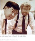
1940年 pn结的发现 Russell Ohl 发现了 p-n 结和硅中的光电效应,从而引起了结型晶体管和太阳能电池的发展。 Russell Ohl in his laboratory at Bell Laboratories 2006-2007 Alcatel-Lucent. All rights 图一 .Russell Ohl 在贝尔实验室里他自己的实验室中 20 世纪三十年代中期,在美国新泽西州霍姆德尔的贝尔实验室里,一位名为 Russell Ohl 的电化学研究者开始研究硅整流器作为雷达探测器的应用。他发现提高硅的纯度有助于提升它们的探测能力。 1940 年 2 月 23 日 ,他测试的一片硅片表现异常,展示出令人吃惊的结果。当暴露于强光中时,流过硅板的电流轻微地跳动了一下。同时他发现,当用“猫须”探针测试时,晶体的不同部分表现出相反的电场效应。 Ohl 和同事 Jack Scaff 发现硅板上的一个接缝把硅板分成了两个不同的部分,每一部分分别含有不同的杂质。一种杂质是 P 元素,它导致所测样品结构中的电子含量稍微过量;另一种是 B 元素,它导致电子含量略微不足(后来被称为“空穴”)。他们把这两个区域称为 n 型(负极)和 p 型(正极);这两个区域相交的界面或者说“隔阂区”,成为众知的“ p-n 结”。光照射到结上,激发出电子,从 n 极流向 p 极,形成电子流。 Ohl 发现光电效应,给今天的太阳能板( 1954 里程碑)提供了能源。 William Shockley 在 1948 年定义的结型晶体管的概念( 1948 里程碑)就来源于 Ohl 在 1940 年的偶然发现。p -n 结成为了电子产业里最通用的整流器,并且从此成为了半导体器件设计中的一种基本元器件。 Excerpt from Rusell Ohl's notebook entries of February 21, 1940 2006-2007 Alcatel-Lucent. All rights reserved 图二 .Rusell Ohl 在 1940 年 2 月 21 日 的笔记内容的部分摘录 Figures 8 - 13 from Ohl patent filed in 1941 U. S. Patent Office 图三 . 图片 8-13 摘自 Ohl 的收录于 1941 年的专利 同期文献 Ohl,R.S. 《光敏电器》 美国专利 2402662 (收编于 1941 年 5 月 27 日 ,发行于 1946 年 6 月 25 日 )。 Shaff,J.H. Ohl,R.S. 《应用于微波雷达接受器的硅晶体整流器的发展》,贝尔系统工艺期刊, 26 期( 1947 ),第 1 页 口述历史 电气工程师 Ohl,Russel S. 于 1975 年在 Frank Polkinghom 的指引下口述历史。 Frank Polkinghom 是美国新泽西州新不伦瑞克区的罗格斯大学里 IEEE( 译者注:电器和电子工程师协会 ) 成员。 “ Lillian Hoddeson 对 Russell Ohl 的口述历史访问”,( 1976 年 8 月 19-20 )玻尔图书馆及档案馆和美国物理研究所分部的物理学史中心。 更多信息 Riordan,Michael 和 Hoddeson, Lillian ,《 p-n 结的起源》, IEEE 系列( 1997.6 ),页 46-51. Riordan, M 以及 Hoddeson, L. Crystal Fire : 《信息时代的诞生》(纽约: W. W. Norton, 1997 ),页 88-98. Russell Ohl (bow tie) with Jack Scaff (dark hair) at Bell Laboratories Courtesy of: Bell Laboratories and AIP Emilio Segre Visual Archives 图四 . Russell Ohl (蝴蝶结领结)和 Jack Scaff (黑头发)在贝尔实验室 译者:哈尔滨工业大学(威海)电子封装 090840106- 王青 校对:哈尔滨工业大学(威海)电子封装 090840104-李涵竹 原文 http://www.computerhistory.org/semiconductor/timeline/1940-Discovery.html 版权 copyright bywww.computerhistory.org 1940 — p-n 结的发现 Russell Ohl discovers the p-n junction and photovoltaic effects in silicon that lead to the development of junction transistors and solar cells. In the mid-1930s Russell Ohl, an electrochemist at Bell Telephone Labs in Holmdel, NJ, began investigating the use of silicon rectifiers as radar detectors . He found that increasing the silicon purity helped improve their detection ability. On 23 February 1940, he tested a small silicon slab that yielded strange, surprising results. When exposed to bright light, the current flowing through the slab jumped appreciably. He also noticed that different parts of the crystal yielded opposite electrical effects when tested with a " cat’s whisker " style probe. Ohl and colleague Jack Scaff found that a seam in the slab marked the separation of the silicon into regions containing distinct kinds of impurities. One impurity, the element phosphorus, yielded a slight excess of electrons in the sample while the other, boron, led to a slight deficiency (later recognized as "holes"). They called the regions n -type (for negative) and p -type (positive); the surface or "barrier" where these regions met became known as a " p-n junction." Light striking this junction stimulated electrons to flow from the n -side to the p -side, resulting in an electric current. Ohl had discovered the photovoltaic effect that powers today’s solar cells ( 1954 Milestone ). William Shockley’s conception of the junction transistor in 1948 ( 1948 Milestone ) derived from Ohl’s serendipitous 1940 discovery. The p-n junction became the most common form of rectifier used in the electronics industry and has since become a fundamental building block in the design of semiconductor devices. Contemporary Documents Ohl, R.S. "Light-Sensitive Electric Device" U. S. Patent 2402662 (Filed May 27, 1941, Issued June 25, 1946). Shaff, J. H. Ohl, R.S. "Development of silicon crystal rectifiers for microwave radar receivers," Bell System Technical Journal Vol. 26 (1947) p. 1 Oral Histories Ohl, Russel S. Electrical Engineer, an oral history conducted in 1975 by Frank Polkinghorn, IEEE History Center, Rutgers University, New Brunswick, NJ, USA. "Oral history interview of Russell Ohl by Lilllian Hoddeson," (August 19-20, 1976) The Niels Bohr Library Archives and the Center for History of Physics, Divisions of the American Institute of Physics. More Information Riordan, Michael and Hoddeson, Lillian . "The Origins of the pn Junction," IEEE Spectrum (June 1997) pp. 46-51. Riordan, M Hoddeson, L. Crystal Fire: The Birth of the Information Age. (New York: W. W. Norton, 1997 ) pp. 88-98.
1960年外延沉积过程中提高晶体管的性能 薄膜晶体生长过程的发展,导致具有高转换速度的晶体管。 1951年,戈登舠尔和霍华德克里斯滕森在贝尔实验室开发的一个现在被称为外延沉积过程,此过程成长在基板上,继续底层基板上成长一层薄的材料晶体结构。 sheftal',Kokorish,和Krasilov在苏联1957年描述过硅和锗类似的工作过程。 在伊恩圠斯的敦促下,1960年由亨利瘠鶖尔领导的贝尔实验室团队用化学气相沉积增加基层和晶体管集电极之间的薄硅外延层。这种方法不仅提高了晶体管的击穿电压同时显著提高了开关速度(1961年的里程碑)这两个重要的电路设计特点。额外的工艺步骤添加的制造成本比被设备改善的性能还要多。这项技术很快的传到了西方电气公司,并在通过贝尔系统转换的电子电话硅晶体管的制造业中使用。 陶依尔的一个外延晶体管的介绍在1960年6月的固态设备研究会议引起了广泛的关注。 Fairchild公司用外延工艺制造的2N914,在1961年3月推出其最成功之一的晶体管,并迅速被Rheem, Sylvania和Texas仪器公司效仿。 摩托罗拉将此工艺应用在大规模生产汽车交流发电机设备过程中, 硅外延工艺在早期双极集成电路制造业产量的重要影响,使个别电路元件电气隔离的完成更加容易。后来广泛应用在MOS产品制造生产中。外延生长技术也常用在形成超薄层的复合半导体制造中。 图一 伊恩罗斯作为贝尔实验室的董事长的素描像 Pencil sketch of Ian Ross as president of Bell Labs 2006-2007 Alcatel-Lucent. All rights reserved 图2 单一外延工艺反应装置图 Diagram of a simple epitaxial reactor 2006-2007 Alcatel-Lucent. All rights reserved 图3 在运行当中的外延反应装置研究模型图 A research-scale epitaxial reactor in operation Credit: University of South Carolina 图4 外延晶体管在贝尔数字切换系统的应用图 Epitaxial transistors were used in the Bell Number One ESS switch Credit: ATT Corporate History 译者:哈尔滨工业大学(威海)电子封装 090840128-徐涛 校对:哈尔滨工业大学(威海)电子封装 090840127-周超 原文 http://www.computerhistory.org/semiconductor/timeline/1960-Epitaxial.html 版权 copyright by www.computerhistory.org 1960 - Epitaxial Deposition Process Enhances Transistor Performance Development of thin-film crystal-growth process leads to transistors with high switching speeds. In 1951 Gordon Teal and Howard Christensen at Bell Labs developed a process, now called epitaxial deposition, to grow a thin layer of material on a substrate that continues the underlying crystalline structure. Sheftal’, Kokorish, and Krasilov described similar work on germanium and silicon in the U.S.S.R. in 1957. At the urging of Ian Ross, a Bell Labs team led by Henry Theurer used chemical-vapor deposition to add a thin epitaxial layer of silicon between the base and collector of a transistor in 1960. This approach raised the transistor’s breakdown voltage while dramatically increasing its switching speed, (1961 Milestone) two important circuit-design characteristics. The added manufacturing cost of the extra process step was more than offset by improvements in device performance. The technology was quickly transferred to Western Electric and used in manufacturing silicon transistors for electronic telephone switching in the Bell System. Theurer gave a presentation on epitaxial transistors at the June 1960 Solid-State Device Research Conference that aroused widespread interest. Fairchild used epitaxy to fabricate the 2N914, one of its most successful transistors introduced in March 1961 and quickly emulated by Rheem, Sylvania, and Texas Instruments. Motorola applied the process to mass produce devices for automotive alternators. Epitaxial silicon also had an important impact on the manufacturing yield of early bipolar integrated circuits by allowing electrical isolation of the individual circuit components to be accomplished much more easily. It later found widespread application in the manufacture of MOS products. Epitaxial growth techniques are also used to form the ultra-thin layers common in compound-semiconductor manufacturing.
1961- 硅晶体管超过锗晶体管的速度 计算机工程师 西摩 · 克雷基金发展第一个硅装置来满足世界上最快机器的性能要求。 在通用自动电子计算机方面,计算机工程师西摩 · 克雷曾经致力于通用晶体管公司的锗晶体管。在和 威廉 · 诺里斯一成立数据控制公司,克雷就让通用晶体管公司为 CDDC 1604 计算机生产出了快速切换的锗设备,这个计算机在 1960 年成为了第一个商业成功的大型科学计算晶体管机器。 为了创造世界上最快的超级计算机,克雷要求一个在成百上千设备近距离工作产生的高温环境中运行且能在 3 纳秒之内切换的晶体管。 克雷授予飞兆半导体公司 500 , 000 美元的开发合同要为 CDC 6600 制造一个新的晶体管。 吉恩 · 赫尔尼达到了技术要求,结合 “ 掺金 ”—— 除了黄金杂质 - 连同新的外延沉积过程。该 2n709 ( ft-1310npn 型装置)在 1961 年 7 月作为第一类超越锗速度的硅晶体管被介绍推出。 每一个 CDC 6600 用 600 , 000 个晶体管封装在一个独特的 cordwood-style 模块配置中来减少连接电线的长度。在 1964 年飞兆半导体因为超过一千万的设备被成为“半导体产业历史上最大的单一指令之一”。科学数据系统是另一个在西格玛系列电脑逻辑应用中高速硅半导体的早期采纳者。 Jean Hoerni working in the lab 图片 1 :吉恩 · 赫尔尼正在实验室工作。 。 2N709 die - epitaxial gold-doped switching transistor 图片 2 : 2N709 晶圆外延开 掺金开关晶体管。 CDC 6600 "cordwood-module" transistor-based logic units 图片 3 : CDC 6600”cordwood 模块 ” 电晶体逻辑组合。 Open logic and memory "leaves" of a CDC 6600 图片 4 : CDC 6600 的开放式逻辑与记忆的“叶子”。 版权 copyright by www.nobeprize.org 译者:哈尔滨工业大学(威海)电子封装 090840129-祝乐 校对:哈尔滨工业大学(威海)电子封装 090840112-李迪 1961 - Silicon Transistor Exceeds Germanium Speed Computer architect Seymour Cray funds development of the first silicon device to meet the performance demands of the world’s fastest machine. Computer architect Seymour Cray had worked with General Transistor Corporation’s germanium transistors at Univac. On founding Control Data Corporation in 1957 with William Norris, Cray asked General Transistor to develop a fast switching germanium device for the CDC 1604 that in 1960 became the first commercially successful large-scale transistor machine for scientific computing. With the goal of building the world’s fastest supercomputer, Cray required a transistor that switched in less than 3 nanoseconds while operating in a high temperature environment created by hundreds of thousands of devices operating in close proximity. Early silicon transistors offered superior operation to germanium at elevated temperature but were too slow for many computer designs. Cray awarded Fairchild Semiconductor a $500,000 development contract to build a new transistor for the CDC 6600. Jean Hoerni met the specification by combining "gold-doping" - the addition of gold impurities - together with the new epitaxial deposition process. ( 1960 Milestone ) The 2N709 (FT-1310) n-p-n device was introduced in July 1961 as the first silicon transistor to exceed germanium speed. Each CDC 6600 used 600,000 transistors packaged in a unique cordwood-style module configuration to minimize connecting wire lengths. In 1964 the company placed "one of the largest single orders in the history of the semiconductor industry" with Fairchild for over 10 million devices. Scientific Data Systems was another early adopter of high-speed silicon transistors for logic applications in the Sigma series computers.
1963年标准逻辑集成电路家族介绍 二极管 - 晶体管逻辑电路 (DTL) 家族为数字集成电路创造了广大的市场,但是到二十世纪六十年代末期在速度,成本及集成度方面占优势的改进型肖特基晶体管(TTL)成为了最流行的标准逻辑配置。 分离二极管 - 晶体管逻辑电路 (DTL) 的完整版本成为了第一个大量 IC 产品生产线。贝克·奥威尔在 1962 年设计的, se100 系列的 DTL 家族被 Fairchild 的 930 系列创造的一个有竞争力的跳背模式产品以其更小的噪音,更便宜的价格优势所赶超,这种产品一直沿用至今。 Pacific Semiconductor 的 James Buie 在 1961 年申请专利, TTL (晶体管—晶体管逻辑电路)作为以后二十年里最受欢迎的逻辑配置出现。没有注意到 Bule 的成果,但是因为 Ruegg 和 Fairchild 的 Beeson 描绘的“完全晶体管”逻辑电路模型而有了灵感, Thomas Longo 在 1963 年领导设计了第一个 TTL 家族——西尔维尼亚万能高电平逻辑电路( SUHL )。被 SUHL 在凤凰导弹应用的成功所激励, TI 在第二年生产了有竞争力的 TTL 家族的 SN5400 系列 。这个公司在 1966 年发布的 SN7400 系列是为工业顾客设计的低成本的塑料封装,它迅速占领了逻辑领域超过百分之五十的市场。 到 1968 年,平板印刷术很大的增加了整合在芯片上的晶体管的数量,热切地希望在 TTL 产业占一定的份额, Fairchild ( 9300 系列)和 Signetics ( 8200 系列)开拓了 TTL-MSI (中等规模集成—每个芯片上升至 100 个逻辑入口) 结的设计制造,比如计数器,注册转移和算术逻辑部件。一些卖家应用萧特基( 1969 年的里程碑)和互补型金属氧化物半导体( 1963 年的里程碑)技术去建立更大,更快,耗能更低的 TTL 兼容结,它拓宽了有效年限和这种受欢迎的逻辑配置的申请范围。 Introduced 2 years after Signetics SE124 DTL flip-flop, Fairchild's 930 series DTL (right) was smaller and therefore cheaper and faster Credit: Fairchild Camera Instrument Corporation Signetics的SE124DTL触发器引入两年后,Fairchild的930系列DTL更小因此成本更低更快 Dr. Thomas A. Longo developed SUHL TTL at Sylvania in 1963 Credit: Fairchild Camera Instrument Corporation Thomas A. Longo博士于1963年在西尔维尼亚研制了SUHL TTL The indispensable data manual of the 1970s Courtesy of: Texas Instruments, Inc 1970系列必不可少的的数据手册 Am9300 TTL MSI universal shift register. AMD’s first product was an improved version of the Fairchild original CHM Collection. Photo gift of Ed Turney Am9300 TTL MSI 的通用转换缓存器,AMD的第一个产品是一个Fairchild原始版本的改进版 译者:哈尔滨工业大学(威海) 电子封装 090840204-马聪 校对:哈尔滨工业大学(威海)电子封装 090840206-杨英坤 原文: http://www.computerhistory.org/semiconductor/timeline/1963-TTL.html 版权 copyright by www.computerhistory.org 1963 - Standard Logic IC Families introduced Diode Transistor Logic (DTL) families create a high-volume market for digital ICs but speed, cost, and density advantages establish Transistor Transistor Logic (TTL) as the most popular standard logic configuration by the late 1960s. Integrated versions of discrete diode transistor logic (DTL) circuits became the first high-volume IC product lines. Designed by Orville Baker in 1962, the Signetics SE100 Series DTL family was overtaken in 1964 by the better noise immunity and lower cost of Fairchild's 930 Series establishing a competitive industry leap-frog pattern that continues today. Patented by James Buie of Pacific Semiconductor in 1961, TTL (Transistor Transistor Logic) emerged as the most popular logic configuration of the next two decades. Unaware of Buie's work but inspired by an "all transistor" logic circuit described by Ruegg and Beeson of Fairchild, Thomas Longo led the design of the first TTL family, Sylvania Universal High-level Logic (SUHL) in 1963. Encouraged by SUHL's success in winning a high-profile Hughes military design (the Phoenix missile), TI introduced the competing SN5400 Series TTL family the following year. The company announced the SN7400 Series in low cost plastic packages for industrial customers in 1966 and quickly gained a greater than 50% share of the logic market. By 1968 lithography advances significantly increased the number of transistors that could be integrated on a chip. Eager to win a share of the TTL business, Fairchild (9300 Series) and Signetics (8200 Series) pioneered the design of TTL-MSI (Medium Scale Integration - up to 100 logic gates per chip) functions such as counters, shift registers, and arithmetic logic units. Many vendors applied Schottky ( 1969 Milestone ) and CMOS ( 1963 Milestone ) technology to build larger, faster, and lower power TTL-compatible functions that extended the useful life and range of applications of this popular logic configuration.
半导体里程 _ 博物馆 _ 第一个商业MOS集成电路的介绍 Andy Grove, Bruce Deal, and Ed Snow discuss MOS technology at the Fairchild Palo Alto R D laboratory in 1966 Credit: Fairchild Camera Instrument Corporation 图一 安迪 · 格鲁夫 , 布鲁斯 · 帝尔 , 艾德 · 雪飞在帕洛阿尔托的飞兆半导体研发实验室探讨 MOS 技术于 1966 年 一般微电子使用一种金属氧化物半导体 (MOS) 处理来在芯片上装比双极集成电路更多的晶体管,并使用这项技术建立了第一个计算器芯片组。 由于复杂的制造和可靠性问题,所以实现 MOS 关于比双级( 1960 里程碑)高密度和低成本的承诺比预期的更困难。在研讨会上的发言者把在电子学方面的失败的物理现象与盲人摸象的故事做比较 -— 这主要取决于你检查哪一部分。 1961 年弗雷德里克· 海曼 和史蒂文·奥弗斯坦在美国无线电公司做了个关于 16 晶体管集成电路的实验并且后来在了解表面氧化物质量方面做出了重要贡献。在 1963 年和 1966 年之间,布鲁斯·帝尔,安德鲁·格鲁夫和艾德·雪尔在仙童 半导体公司 鉴定了纳污染问题并且出版了很多关于氧化物的电性性质的论文这些为格鲁夫的经典教材《物理和半导体设备技术》提供了资料。世界各地的合作与竞争,包括来自 NEC · IBM ·飞利浦的研究者在最后的十年中解决了基本的产量和可靠性问题使得 MOS 作为主导的 IC 技术出现。 R. P. Donovan’s illustration of the spectrum of MOS instability explanations presented at a 1966 symposium Courtesy of: Bruce Deal and Harry Sello 图二 R.P 多诺万的关于 MOS 不稳定性的图解在 1966 年的一个研讨会上呈现 The first commercial MOS IC, GMe's 20-bit shift register used 120 p-channel transistors in 1964 CHM Collection. Photo gift of Don Farin 图三 第一个用了 120 个通道的 晶体管的商用 MOS IC 、 GMe 的 20-bit 移位寄存器在 1964 年 1964 年当罗伯特·诺曼使用一个二阶段时钟计划来设计一个用 120p 通道晶体管的 20 位移位寄存器时,普通的微电子推出了第一个商业 MOS 集成电路。 1965 年, GMe 作为第一个基于 MOS 的电子计算操纵者为 维克特康普托计算机 设计了 23 位自定义集成电路。 飞哥福特 收购了该公司并且将业务转移到费城大多数员工转移到其他公司后,在 航空英里指示器 及通用仪器方面继续蓬勃发展计算机芯片市场。 The prototype Victor Comptometer EC-3900 calculator and board with 23 custom MOS chips and six 100-bit shift registers for serial memory CHM Collection. Gift of Don Farina 图四康普托计算机原型 EC- 3900 计算器和在 23 个自定义 MOS 芯片和六个 100 位移位寄存器和串行存储器 到 1969 年罗克韦尔微电子学为夏普的第一台便捷携带式机 microCompet QT-8D 已经将电子芯片数降到四台设备,并且继续前进成为上世纪 70 年代早期的计算机芯片最大供应商。 1971 年 泰克 及 美国德州仪器公司(1974 里程碑 ) 介绍了单片机 ( 除了外部显示器 ) 驱动程序解决方案 。 译者:哈尔滨工业大学(威海)电子封装 090840206- 杨英坤 校对:哈尔滨工业大学(威海)电子封装 090840204 马聪 原文 http://www.computerhistory.org/semiconductor/timeline/1964-Commecial.html 版权 copyright by www.computerhistory.org ——————————————————————— 1964 - First Commercial MOS IC Introduced General Microelectronics uses a Metal-Oxide-Semiconductor (MOS) process to pack more transistors on a chip than bipolar ICs and builds the first calculator chip set using the technology Achieving the MOS promise of higher density and lower cost than bipolar ( 1960 Milestone ) proved more difficult than anticipated due to complex manufacturing and reliability issues. Speakers at a symposium on the Physics of Failure in Electronics likened competing solutions to the story of the blind man and the elephant – it depends on which part you examine. Frederic Heiman and Steven Hofstein built an experimental 16-transistor IC at RCA in 1961 and later made important contributions to understanding surface oxide quality. Between 1963 and 1966, Bruce Deal, Andrew Grove, and Ed Snow at Fairchild identified the issue of sodium contamination and published many papers on the electrical nature of oxides that informed Grove’s classic textbook Physics and Technology of Semiconductor Devices. Collaboration and competition across the globe, including researchers from NEC, IBM and Philips, resolved the fundamental yield and reliability issues by the end of the decade that allowed MOS to emerge as the dominant IC technology. General Microelectronics introduced the first commercial MOS integrated circuit in 1964 when Robert Norman used a 2-phase clock scheme to design a 20-bit shift register using 120 p-channel transistors. GMe designed 23 custom ICs for the first MOS-based electronic calculator for Victor Comptometer in 1965. After the company was purchased by Philco-Ford and the operation transferred to Philadelphia most employees moved on to other companies, including AMI and General Instrument, where they continued to develop chips for a burgeoning calculator market. By 1969 Rockwell Microelectronics had reduced the chip count to four devices for Sharp's first portable machine, the microCompet QT-8D , and went on to become the largest supplier of calculator chips in the early 1970s. Mostek and TI ( 1974 Milestone ) introduced single-chip (except for external display drivers) solutions in 1971.
1964 年 - 第一个被广泛使用的模拟集成电路出现 大卫塔尔伯特和罗伯特维德勒在飞兆半导体通过建立商业上成功的模拟应用集成电路,开启了一个主要行业部门。 模拟,也称为线性电路,像声音,温度和无线电波那样电路放大和状态信号不断变化的现象。由于处理这些信号需要极高的分辨率,模拟电路要求在设计和制造中有很高的精度。模拟电子管运放的设计是由哥伦比亚大学的研究员露比朱莉的想法一步一步开发的。第一个锗晶体管运放出现在 1958 年,硅晶体管出现在 1960 年。在布尔布朗和菲尔布里克的研究之后不久 nexus 研究室于 1962 年推出第一个预配置的运放模块 。 艾米克,飞兆半导体,莲花,德州仪器和西屋电气公司开发了早期的模拟集成电路。西屋电气公司的林慧聪 1963 年在 Autonetics 民兵 2 导弹的传统运放上使用了片状元件匹配和外侧三极管专利。但是 1964 年由飞兆半导体公司的工艺工程师戴维卡尔伯特和设计师罗伯特韦德的团队发明的 μA702 运放才是第一个被广泛使用的商业产品。 1965 年的继承者 μA709 运放为模拟集成电路建立了巨大的市场。塔尔伯特和韦德在 1965 年末搬到 molectro (后来被国家收购),在那他们通过 lm101 开始建立了一个长久的王朝。然后在 1968 年飞兆半导体的戴维富嘉通过增加一个固有补偿电容第一次升级了 lm101 ,得到 μA741 ,这是有史以来最流行运放。 专业模拟集成电厂商为放大器,比较器,数据转换器,电源管理器件,和汽车,消费,通信应用周边的大量特点发展了广泛的产品目录。模拟器件通常比数字集成电路具有更长的寿命周期。例如有四十年历史的富嘉的 μA741 运放,汉斯 Camenzind Signetics 公司制造的 555 定时器在今天仍被广泛应用。 Robert Widlar inspects the LM10 mask layout circa 1977 Credit: National Semiconductor 罗伯特 · 维德拉 1977 年检查 LM10 版图 An early analog IC, the Fairchild μA700 differential amplifier designed by Bohumil Polata (1963) Credit: Fairchild Camera Instrument Corporation 早期的模拟集成电路,飞兆半导体的 μA700 : Bohumil Polata ( 1963 )设计的差分放大器 Talbert and Widlar's μA709 high-performance operational amplifier (1965) Credit: Fairchild Camera Instrument Corporation 塔尔伯特和维德拉的 μA709 高性能运算放大器( 1965 ) Widlar's LM10 op amp broke new ground for low voltage operation Credit: National Semiconductor 维德拉的 LM10 运算放大器打破了低电压差工作的新局面 译者:哈尔滨工业大学(威海)电子封装 090840207-邹运 校对:哈尔滨工业大学(威海) 原文 http://www.computerhistory.org/semiconductor/timeline/1964-analog.html 版权 copyright by www.computerhistory.org —————————————————————————————————————————————————— 1964 - The First Widely-Used Analog Integrated Circuit is Introduced David Talbert and Robert Widlar at Fairchild kick-start a major industry sector by creating commercially successful ICs for analog applications. Analog, also called linear, circuits amplify and condition signals from continually varying phenomena such as sound, temperature, and radio waves. Because of the nearly infinite resolution required to process these signals, analog circuits demand high precision in design and manufacturing. Analog vacuum tube operational amplifier (op-amp) designs were paced by the concepts developed by Columbia University researcher Loebe Julie. The first germanium transistor op-amp appeared in 1958 with silicon versions in 1960. Nexus Research Labs offered the first pre-configured op-amp modules in 1962 followed shortly by Burr-Brown and Philbrick Researches. Amelco, Fairchild, RCA, TI, and Westinghouse developed early analog ICs. H. C. Lin of Westinghouse employed on-chip component matching and his lateral PNP patent on a custom op amp for the Autonetics Minuteman II missile in 1963. But the Fairchild μA702 op amp, created in 1964 by the team of process engineer Dave Talbert and designer Robert Widlar, was the first widely-used commercial product. Their 1965 successor, the μA709, established a mass market for analog ICs. Talbert and Widlar moved to Molectro (later acquired by National) in late 1965 where they built a linear dynasty beginning with the LM101. Then in 1968 Dave Fullagar of Fairchild one-upped the LM101 by adding an internal compensating capacitor to deliver the μA741, the most popular op-amp of all time. Specialty analog IC manufacturers evolved extensive catalogs of amplifiers, comparators, data converters, power management devices, and numerous specialty circuits for automotive, consumer and communications applications. Analog devices typically have much longer life cyles than digital I/Cs. Examples of 40 year-old designs that remain widely used today include Fullagar's μA741 op-amp and the 555 timer created by Hans Camenzind for Signetics.
1965“摩尔定律”预测 集成电路的发展走向 戈登·摩尔,飞兆半导体公司的研发总监,在一篇内部文献中作了一张图,图中有一条通过五个点的线,代表着1959年至1964年间每片集成电路中一个元器件所需成本的变化情况。摩尔在《集成电子学的未来》这一文献中试图预测未来十年里集成电子学最可能的发展情况。当摩尔以每12个月器件数量翻一番的发展趋势在投影图上进行推断,他发现1975年每个芯片上的器件数目会达到65000个。《让集成电路填满更多元件》作为一篇杂志文章,于1965年4月19日发表在《电子》杂志上。 Gordon Moore at Fairchild R D in 1962 1962年戈登·摩尔在飞兆半导体公司研发中心 Credit: Fairchild Camera Instrument Corporation 在1975年的国际电子器件会议中,摩尔指出光刻方法,晶圆尺寸,工艺技术的发展,以及设备与装置的智能化,尤其是半导体存储器阵列化,能使他发现的规律得意现实。根据更多的近期数据,其中包括更高复杂程度(仅仅比存储器密度低)的微处理器设计,摩尔把未来器件复杂度的增加速率从一年翻一番降为两年翻一番。 Cost vs. time sketch from Moore's 1964 notebook 1964年,戈登·摩尔笔记本中成本与时间关系的草图 Credit: Fairchild Camera Instrument Corporation 这个预测成为一个自我实现的预言,成为半导体工业遵守的一个法则。专家指出年度突破挑战,以确保符合由卡弗·米德命名的“摩尔定律”。1995年,再次回顾产业现状时 (此时英特尔奔腾处理器含有近500万晶体管),摩尔说,“当前的预测是,这样的发展不会马上停止。”一个装置(美国)含有超过十亿个晶体管。 Dr. Moore revisits his projection with additional data gathered through 1975 摩尔博士获取1965年至1975年的新数据之后重新制作的投影图 Courtesy of: Intel Corporation Several of the chips in this photo provided data points for the 1965 article 图中的芯片为1965年发表的那篇文献提供了数据 Credit: Fairchild Camera Instrument Corporation 译者:哈尔滨工业大学(威海)电子封装 090840208-汪洋 校对:哈尔滨工业大学(威海)电子封装 090840209-常青 原文 http://www.computerhistory.org/semiconductor/timeline/1965-Moore.html 版权 copyright by www.computerhistory.org —————————————————————————————————————————————————————— 1965 - "Moore's Law" Predicts the Future of Integrated Circuits Fairchild’s Director of R D predicts the rate of increase of transistor density on an integrated circuit and establishes a yardstick for technology progress. Gordon Moore, Fairchild Semiconductor’s Director of RD, wrote an internal paper in which he drew a line through five points representing the number of components per integrated circuit for minimum cost per component developed between 1959 and 1964. "The Future of Integrated Electronics" attempted to predict "the development of integrated electronics for perhaps the next ten years." Extrapolating the trend to 1975 he projected that the number of components per chip would reach 65,000; a doubling every 12 months. Edited for publication as a magazine article, "Cramming more components onto integrated circuits" was published in Electronics on April 19, 1965. At the 1975 IEEE International Electron Devices Meeting Moore, by now with Intel, noted that advances in photolithography, wafer size, process technology, and "circuit and device cleverness," especially in semiconductor memory arrays, had allowed his projection to be realized. Adding more recent data, that included a higher mix of microprocessor designs that were somewhat less dense than memories, he slowed the future rate of increase in complexity to "a doubling every two years, rather than every year." This prediction became a self-fulfilling prophecy that emerged as one of the driving principles of the semiconductor industry. Technologists were challenged with delivering annual breakthroughs that ensured compliance with "Moore’s Law," as it was dubbed by Carver Mead. On reviewing the status of the industry again in 1995 (at which time an Intel Pentium microprocessor held nearly 5 million transistors) Moore concluded that “The current prediction is that this is not going to stop soon.” Devices exceeding one (U.S.) billion transistors exist today.
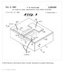
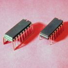
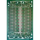
1965- 封装成为系统设计首要问题 摘要: 双列直插的封装格式显著简化 PCB 板布局并降低计算机的组装成本 大多数半导体器件采用陶瓷,金属或塑料等封装形式密封以防止芯片和脆性连接线的损坏。封装工艺尽管具有这样重要的功能,在半导体设计中却是最被疏忽的方面,芯片尺寸过大和功耗过多一直阻碍着封装进程发展。典型的 60 年代的三极管都采用的是带有 3 条外引线的 TO-5 或者 TO-18 金属罐封装。低成本的塑料形式主要用于气密性要求不高的产品,飞兆半导体第一次在最多容纳 10 条外引线的晶体管罐子上安装了微逻辑集成电路。为使航空电子设备上的芯片占有面积最小化,德州仪器的陶荣开发了一种 10 引线 0.25 , ,0125 英寸的扁平封装形式。 · 这些封装迭代大多数源自于现有格式,并不适用于高密度电路板的设计。 1965 年,飞兆半导体的 Don Forbes, Rex Rice, and Bryant ("Buck") Rogers 等人设计了一种 14 引线的,两侧带有 100 密尔的引脚的双列直插式封装形式,这样设计既简化了电路板的布局,又使得器件可自动插入 PCB 板,因此造就了一次计算机制造业的革命。 70 年代前期,低成本,塑料成型版的双列直插封装产量主导了整个产业,并且引脚数一直增加到 64 · 虽然大多数的 DIP 设计采用热压或超声波焊接到纯金或铝导线的芯片,一些厂商尝试用马丁 · 贝尔实验室 Lepselter 发明的微小的焊料凸点互连和改变光束引脚链接的方法,用于高可靠性的应用 前后修边的玻璃密封陶瓷双列直插封装 塑料DIP半剖示意图 摩托罗拉和德州仪器在DEC AXC板上安装的20引脚封装芯片 AMD公司在80年代中期的不同外形的DIP封装 译者:哈尔滨工业大学(威海)电子封装 090840210 高阳 校对:哈尔滨工业大学(威海) 原文 http://www.computerhistory.org/semiconductor/timeline/1978-PAL.html 版权 copyright by www.computerhistory.org 1965 - Package is the First to Accommodate System Design Considerations The Dual In-line Package (DIP) format significantly eases printed circuit board layout and reduces computer assembly cost. · Most semiconductor devices are enclosed in ceramic, metal or plastic packages to prevent damage to the chip and its fragile connecting wires. Despite this important function, packaging was one of the most neglected aspects of semiconductor design. Programs were delayed because the chip was too large or consumed too much power for the designated package. Typical 1960s transistors used TO-5 or TO-18 (Transistor Outline) metal-can packages with three external leads. Lower-cost plastic versions served applications not requiring a hermetic seal . Fairchild mounted its first Micrologic ICs in such transistor cans modified to accommodate up to 10-leads. Yung Tao at Texas Instruments developed a 10-lead, 0.25 by 0.125 inch flat-pack to occupy the smallest possible board area in avionics systems. · Most of these package iterations were derived from existing formats that were not conceived for high-density board designs. In 1965 Don Forbes, Rex Rice, and Bryant ("Buck") Rogers at Fairchild devised a 14-lead ceramic Dual-in-Line Package (DIP) with two rows of pins 100 mils apart that revolutionized computer manufacturing by simplifying layout and allowing automated insertion into printed circuit boards. Low-cost, plastic-molded versions of the DIP outline dominated production volumes by the early 1970s and pin-counts increased up to 64 leads. · While most DIP designs used thermo-compression or ultrasonic bonding to attach fine gold or aluminum wires to the chip, some vendors experimented with tiny solder bump interconnects and variations on a beam-lead approach invented by Martin Lepselter of Bell Labs for high-reliability applications.
设计创新,提高速度和降低能耗的行业标准的 64 位晶体管内存架构。迅速应用到新的双极逻辑和存储器的设计。 自 1963 TTL ( 1963 里程碑)设备的复杂性,先进的 20 倍,但开关速度保持在每门 10-15 纳秒的延迟相对不变。速度取决于如何快速充电晶体管存储可以去掉。黄金兴奋剂-- 金掺杂 ( 1961 年里程碑)改善,但难以控制。在 1964 年 JR 贝尔德的德州仪器公司( TI )提出使用金属 - 半导体二极管,称为肖特基势垒二极管( 1931 年里程碑) ,分流围绕晶体管的电荷。特德•詹金斯和加思飞兆半导体威尔逊在 1967 年双极型集成电路二极管制造。同时,日本的电工实验室开发出了类似的设计。英特尔设计师理查德•博恩和 H. ţ 蔡氏使用肖特基二极管,在该公司的第一款产品, i3101 64 位的 RAM 的设计。在 1969 年介绍,该装置是较早实现快速的近两倍。 1966 年(里程碑) 在 1971 年 T.I. 推出的 74S 系列 TTL 逻辑系列,采用肖特基二极管,以达到 3 ns 的高速应用的大门延误。低功耗的的肖特基版本,指定的 LS ,迅速取代了原来的 7400 设备,五分之一的电力消耗,提供相同的速度。主席 Mark Shepherd 7400LS 描述为“单一德州仪器的历史中最有利可图的产品线。 ” AMD , Fairchild ,摩托罗拉,国家和 Signetics 也进入了市场。后人,包括 Fairchild 先进的肖特基技术(快速) ,分 2ns 的延迟氧化物隔离工艺相结合的肖特基二极管。 在 70 年代中期,微型可编程位片处理器从 AMD ,英特尔,人机界面,并使用肖特基技术集成 LSI 为高性能运算处理应用的积木 Signetics 公司家庭。 ( 1979 年里程碑) 译者:哈尔滨工业大学(威海)电子封装 090840218赵家玮 原文: http://www.computerhistory.org/semiconductor/timeline/1969-Schottky.html 版权 copyright by www.computerhistory.org The i3101 Schottky TTL 64-bit RAM was Intel's first product 该 i3101 肖特基 TTL64 位内存是英特尔的第一款 Courtesy of: Intel Corporat 74S00 Schottky TTL gate function introduced by TI in 1971 . 74s00 肖特基晶体管晶体管逻辑门功能介绍了钛在 1971 Courtesy of: Texas Instruments, Inc. Introduced in 1975, the Am2901 bit-slice microprocessor used Low-power Schottky (LS) process technology 1975 推出的微处理器, am2901 位片采用低功耗肖特基(镑)工艺技术 Credit: CHM Collection. Gift of John Corbitt Walter Schottky stands between transistor pioneers John Bardeen and Walter Brattain 肖特基•沃尔特站在的先驱约翰巴丁和布拉顿之间 Courtesy of: AIP Emilio Segre Archive, Brattain Collection Since 1963 TTL ( 1963 Milestone ) device complexity had advanced twenty-fold but switching speeds remained relatively unchanged at delays of 10-15 ns per gate. Speed is determined by how quickly charge stored in a transistor can be removed. Gold-doping ( 1961 Milestone ) improved this but was difficult to control. In 1964 J. R. Baird of Texas Instruments (T.I.) proposed using ametal-semiconductor diode, called a Schottky-barrier diode ( 1931 Milestone ), to shunt charge around the transistor. Ted Jenkins and Garth Wilson of Fairchild fabricated such a diode on a bipolar integrated circuit in 1967. Concurrently Japan's Electrotechnical Laboratory developed a similar design. Intel designers Richard Bohn and H. T Chua used a Schottky diode in the design of the company's first product, the i3101 64-bit RAM. Introduced in 1969, the device was nearly twice as fast as earlier implementations. ( 1966 Milestone ) In 1971 T.I. introduced the 74S Series TTL logic family using Schottky diodes to achieve 3 ns gate delays for high-speed applications. Low-power Schottky versions, designated LS, quickly replaced the original 7400 devices by offering the same speed at one fifth the power consumption. Chairman Mark Shepherd described 7400LS as "the single most profitable product line in the history of Texas Instruments." AMD, Fairchild, Motorola, National, and Signetics also entered the market. Later generations, including Fairchild Advanced Schottky Technology (FAST), combined Schottky diodes with oxide-isolation processes for sub-2ns delays. In the mid-1970s micro-programmable "bit-slice" processor families from AMD, Intel, MMI, and Signetics used Schottky technology to integrate LSI building blocks for very high performance arithmetic processing applications. ( 1979 Milestone )
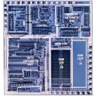
IBM 公司的研究员罗伯特 · 迪纳德关于过程缩放型记忆的论文加速了收缩物理尺寸的全球竞赛和制造更复杂的集成电路。 在 60 年代,每个推进光刻能力面具尺寸的线性收缩提供一个快速解决提高速度和降低成本的集成电路。在 1962 年托马斯斯坦利的研究实验室发表的分析指出,由于其临界速度的极限尺寸,栅极长度,躺在横向而不是纵向平面双极器件,这是特别重要的金属氧化物半导体晶体管。 比例原则在布鲁斯卡弗 · 米德 hoeneisen 和加州理工学院的罗伯特迪纳德和他的同事的 1972 个文件被描述。由于登纳德等的 1974 个文件,引起微电子业界的关注与造成的深远影响。他们指出,由于晶体管的横向尺寸的比例系数,因相同的因素速度得到了提高。当时的 绝缘性场效应管 最小尺寸为 5 微米,他们预计缩小微米组分。(人的头发是 50 - 100 微米直径)这是第一次尝试将几何收缩所产生的结果降低功耗和性能改进。这给戈登穆尔( 1965 年)的 “ 定律 ” 提供了科学基础。 1976 年, MITI 组织公司,富士通日立,三菱、东芝,成一个联盟,超大规模集成电路技术研究协会,包括概念,缩放和结合日本光学和精细的制造优势在 70 年代末在全球范围内提供了 64K 动态随机存取存储器( 1970 的里程碑事件)。在这些高能晶体管上计算的功率消耗加快了 互补金属氧化物半导体 管技术的发展( 1963 的里程碑事件)。 这种尺寸 互补金属氧化物半导体 管的能力在 2006 年末允许尺寸收缩至 100 纳米( 0.1 微米)以下和像 IBM 公司 / 索尼 / 东芝的芯片为第三代游戏机提供了 234000000 个晶体管细胞处理器。 80年代中期IBM研究员 罗伯特· 迪纳德 伴随最小特征尺寸内存单元尺寸的减小 100纳米cmos晶体管的扫描电镜图像 第三代游戏机23000000晶体管细胞处理器 译者:哈尔滨工业大学(威海)电子封装090840224-宁尚佳 校对:哈尔滨工业大学(威海)电子封装 090840227-吴喆熹 原文 http://www.computerhistory.org/semiconductor/timeline/1974-Scaling.html 版权 copyright by www.computerhistory.org ———————————————————————————————— 1974 - Scaling of IC Process Design Rules Quantified IBM researcher Robert Dennard’s paper on process scaling on MOS memories accelerates a global race to shrink physical dimensions and manufacture ever more complex integrated circuits. Linear shrinking of mask dimensions with each advance in lithographic capability provided a quick fix to enhance the speed and reduce the cost of ICs in the 1960s. Thomas Stanley of RCA Research Laboratories published an analysis in 1962 noting that this was particularly relevant to the MOS transistor because its critical speed limiting dimension, the length of the gate, lay in the horizontal rather than the vertical plane of bipolar devices. Scaling principles were described in 1972 papers by Bruce Hoeneisen and Carver Mead of Caltech and by IBM's Robert Dennard and his colleagues. But it was a 1974 paper by Dennard, et. al. that caught the attention of the industry with a resulting profound effect on microelectronics. They noted that as the horizontal dimensions of a transistor were scaled by a factor, speed improved by that same factor. At a time when IBM's MOS memories used a minimum dimension of 5 microns, they projected shrinking to fractions of a micron. (A human hair is 50-100 microns in diameter) This was the first attempt to relate a geometry shrink to the resulting power reduction and performance improvement. It gave Gordon Moore's ( 1965 Milestone ) "Law" a scientific foundation. In 1976 MITI organized Hitachi, NEC, Fujitsu, Mitsubishi and Toshiba into a consortium, the VLSI Technology Research Association, that embraced the concept of scaling and combined it with Japanese optical and ultra-clean manufacturing strengths in a global race to deliver 64K DRAMs ( 1970 Milestone ) by the end of the decade. Power consumption at these high transistor counts accelerated the adoption of CMOS technology. ( 1963 Milestone ) The ability to scale CMOS allowed dimensions to shrink below 100 nanometers (0.1 micron) by 2006 and to deliver chips such as the IBM/Sony/Toshiba 234 million transistor Cell processor for the Playstation 3.
图一 20 世纪 80 年代中期的约翰和 HT 蔡氏 发明单片存储器的约翰和 HT 蔡氏开发了易于使用的可编程阵列逻辑( PAL )和快速原型的定义逻辑功能的设备和工具 创意逻辑设计师意识到,小、快速的 PROM ( 1971 里程碑) ,也可以配置进行简单的逻辑功能。霍尼韦尔要求的基础上,于 1975 年,罗恩·克莱为适合更复杂的逻辑需求适应 Signetics 公司 PROM 电路技术设计了 82S100 可编程逻辑阵列( PLA )。一个所需的功能,表示为布尔逻辑方程,是输入保险丝编程单元,即刻杂设计师的桌面上生成一个定制的 IC 。 约翰和 H.T. 蔡氏与安迪陈在 1978 年推出的一个更精简的架构,他们称为可编程阵列逻辑( PAL ) ,其交易逻辑灵活,有更快的速度和更低的成本。 PALASM ( PAL 汇编)软件设计工具也开发出了易于使用的设备。 License 与 AMD 、国家、 TI 一致将 20 针双极型器件( 16L8 , 16R8 等)确立为行业标准的产品。他们在特雷西基德的一台新机器的灵魂( 1981 年) ,成为一个时代的技术畅销特色。 AMD ( 22V10 )的一个更加灵活的架构 ,来自赛普拉斯和莱迪思的低功率 CMOS 技术,和可重复使用的 CMOS 为基础的 EPROM 器件支持 PC 兼容 Altera 设计原理图输入工具( 1983 年)扩大其应用范围。 赛灵思( 1984 ) ,爱特( 1985 ) , QuickLogic 公司( 1988 )介绍了现场可编程门阵列( FPGA )架构去服务更高的门数的应用。系统设计师选择了统称为 PLD (可编程逻辑器件) ( 1967 里程碑)作为这些用户可配置的首选解决方案超过了所有成本最低或最高性能的应用程序定制的数字逻辑的 ASIC 方法。 图二 MMI PAL16R8 型号的芯片照片 图三 涵盖首次 PAL 应用手册 “ ( 1978 ) 图四 特蕾西基德的普利策奖获奖书 译者:哈尔滨工业大学(威海)电子封装 090840225-石宇辰 校对: 原文 http://www.computerhistory.org/semiconductor/timeline/1978-PAL.html 版权 copyright by www.computerhistory.org ———————————————————————————————— 1978 - PAL User-Programmable Logic Devices Introduced John Birkner and H. T. Chua of Monolithic Memories develop easy-to-use programmable array logic (PAL) devices and tools for fast prototyping custom logic functions. Creative logic designers realized that small, fast PROMs ( 1971 Milestone ) could also be configured to perform simple logic functions. Based on a request from Honeywell, in 1975 Ron Cline adapted Signetics PROM circuit technology to design the 82S100 Programmable Logic Array (PLA) to serve more complex logic needs. A desired function, expressed as set of Boolean logic equations, was entered into a fuse programming unit that instantly generated a custom IC on the designer's desktop. John Birkner and H.T. Chua of Monolithic Memories worked with Andy Chan to introduce a more streamlined architecture they called Programmable Array Logic (PAL) in 1978 that traded logic flexibility for faster speed and lower cost. The PALASM (PAL Assembler) software design tool also made the devices easy to use. License agreements with AMD, National, and TI established the 20-pin bipolar devices (16L8, 16R8, etc) as industry standard products. They are featured in Tracey Kidder’s The Soul of a New Machine (1981), a technology bestseller of the era. A more versatile architecture from AMD (22V10), CMOS technology for lower power from Cypress and Lattice, and reusable CMOS EPROM-based devices supported by PC-compatible schematic-entry design tools from Altera (1983) expanded their range of applications. Xilinx (1984), Actel (1985), and QuickLogic (1988) introduced Field Programmable Gate Array (FPGA) architectures to serve higher gate-count applications. System designers selected one of these user-configurable solutions, collectively known as PLDs (Programmable Logic Devices), over ASIC approaches ( 1967 Milestone ) as the preferred approach to custom digital logic for all but the lowest cost or highest performance application.
贝尔实验室的单芯片DSP-1数字信号处理器设备构架进行了优化,为电子交换系统。 为了能从背景噪声中分离出信息,数字信号处理器( DSP )采用了数学技术来分析来自自然和电子源的模拟信号。转换成数字信号之后,如快速傅立叶变换等算法筛选和重建准备一个可用的模拟信号转换回数据。在音响,通信,图像,雷达,声纳,语音识别系统中,已经实施了 DSP 功能从电子管到集成电路的每一代技术。 在 1970 年,来自 Fairchild 公司( 9334 )和 AMD 公司( 2505 )的 2*4 乘法器作为第一代标准 IC 产品,加快了数学密集型信号处理运算。 TRW 公司的 LSI 产品采用三重扩散双极工艺,建立了更复杂的功能,如 AMD2901 位片在 20 世纪 70 年代后期的视频和国防应用的处理器一起使用的 16x16 乘法器( MPY16 )。 MOS 外围芯片允许信号处理使用通用的微处理器,包括用于摩托罗拉 6800 和英特尔 2920 ( 1979 )的 AMIS2811 ( 1978 ),并结合了可编程的数字信号处理和数据转换电路( 1968 年里程碑)。 单芯片 DSP本质上 是添加了复杂的数学能力的微处理器。贝尔实验室的单芯片 DSP-1 , AT & T 的 ESS 数字交换机的重要组成部分,诞生于 1979 年 5 月。 NEC 的 定点 μ PD7720 ,在 1980 年应用于语音频带,是商业上最成功的早期的 DSP 之一。 TI 的 16 位可编程 DSP 器件的 TMS320 系列从 1983 年开始应用于消费类产品中,从手机到玩具。从 TI 的 集成度更高的 DSP 的连续几代以及 ADI 公司,摩托罗拉,和别人的权力今天的手机,磁盘驱动器, HDTV 产品。 图一: 1979 年贝尔实验室的 DSP-1 设备布局 图二:: 1979 年 TRW 公司的高速乘法累加器的广告 图三::第一的 TMS320 可编程 DSP 器件的芯片的图片 图四::“电子设计”杂志关于 DSP 的专题文章 译者:哈尔滨工业大学(威海)电子封装 090840226-王延博 校对 :哈尔滨工业大学(威海)电子封装 090840216-鞠伯伦 http://www.computerhistory.org/semiconductor/timeline/1979-DSP.html 版权 copyright by www.computerhistory.org 原文 ——————————————————————--------------------------------------------------------------- 1979 - Single Chip Digital Signal Processor Introduced Bell Labs' single-chip DSP-1 Digital Signal Processor device architecture is optimized for electronic switching systems. Digital signal processing (DSP) applies mathematical techniques to analyze analog signals from natural and electronic sources in order to separate information from background noise. After conversion to digital form, algorithms such as the Fast Fourier Transform filter and reconstruct the data ready for conversion back to a useable analog signal. DSP capability has been implemented in every generation of technology from vacuum tubes to ICs in audio, communications, image, radar, sonar, and voice recognition systems. 2 x 4 multipliers from Fairchild (9334) and AMD (2505) in 1970 were among the first standard IC products to speed math-intensive signal-processing algorithms. TRW LSI Products used a triple-diffused bipolar process to build more complex functions, such as the 16x16 multiplier (MPY 16), used together with the AMD 2901 bit-slice processor for video and defense applications in the late-1970s. MOS peripheral chips to enable signal processing using general-purpose MPUs included the AMI S2811 (1978) for the Motorola 6800 and Intel’s 2920 (1979) that combined programmable digital processing and data conversion ( 1968 Milestone ) circuits. Single-chip DSPs are essentially MPUs with added complex math capabilities. Bell Labs’ one-chip DSP-1, a key component of ATT's ESS digital switch, appeared in May 1979. NEC's fixed-point 倀D7720, introduced in 1980 for voiceband applications, was one of the most commercially successful early DSPs. TI’s TMS 320 family of 16-bit programmable DSP devices from 1983 found wide application in consumer products from cell phones to toys. Successive generations of more highly integrated DSPs from TI as well as Analog Devices, Motorola, and others power today's mobile phones, disk drives, and HDTV products.
 标签: 计算机博物馆