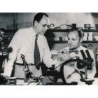
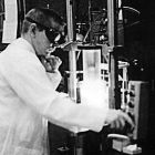
在 威廉 · 肖克利的PN结理论被验证 之后(1948年),制造 一个可以工作的结型晶体管仍然面临严峻的挑战。主要问题是缺乏足够纯净,均匀的半导体材料。贝尔实验室的化学家戈登 · 蒂尔认为,将需要大的单晶,锗和硅, 但听从的人很少,包括 肖克利 。 在管理层很少的支持下, 蒂尔建立自己所需的晶体生长设备, 在 机械工程师约翰小和欧内斯特 · 比埃勒技术员的帮助下。 他在 1917 年由波兰化学家 Jan Czochralski 开发的技术的基础上, 用 一个小的 “ 种子 ” 锗晶体在坩埚熔锗 中 慢慢地缩回来,形成一个狭长的单晶。 肖克利这一成就后来被称为 “ 在初期半导体领域最重要的科学 成果 。 采用这种技术,贝尔实验室的化学家 MorganSparks 通过在 熔融锗晶体生长过程中 加入 微小颗粒杂质,制作 pn 结。 在 1950 年 4 月,他和蒂尔开始向熔体中加入两个连续的小球,第一个是 p 型杂质和第二个是 n 型杂质,形成了内层很薄的 NPN 结构。 一年后,这种 “ 生长出的结型晶体管 ” 超越性能最好的点接触晶体管。 在 1951 年 7 月 4 日, 贝尔实验室在一次 会议 上宣布了这一发现,并强调了肖克利的贡献。 Gordon K. Teal(左)和Morgan Sparks在贝尔实验室,1951年 Morgan Sparks在1949年的第一个结晶体管 2006-2007 Alcatel-Lucent. All rights reserved 1951年,首批微瓦级面结型晶体管中的一只 2006-2007 Alcatel-Lucent. All rights reserve 贝尔M1752型商用结晶体管,约在1951年 Courtesy of: Jack Ward - Transistor Museum 译者:哈尔滨工业大学(威海)电子封装 090840111-计孝智 校对:哈尔滨工业大学(威海)电子封装 090840114-刘继伟 版权 copyright by www.nobeprize.org 原文: http://www.computerhistory.org/semiconductor/timeline/1951-First.html After William Shockley’s theories about p-n junctions had been validated by tests ( 1948 Milestone ), fabricating a working junction transistor still presented formidable challenges. The main problem was lack of sufficiently pure, uniform semiconductor materials. Bell Labs chemist Gordon Teal argued that large, single crystals of germanium and silicon would be required, but few - including Shockley - were listening. With little support from management, Teal built the needed crystal-growing equipment himself, with help from mechanical engineer John Little and technician Ernest Buehler. Based on techniques developed in 1917 by the Polish chemist Jan Czochralski, he suspended a small "seed" crystal of germanium in a crucible of molten germanium and slowly withdrew it, forming a long, narrow, single crystal. Shockley later called this achievement "the most important scientific development in the semiconductor field in the early days." Employing this technique, Bell Labs chemist Morgan Sparks fabricated p-n junctions by dropping tiny pellets of impurities into the molten germanium during the crystal-growing process. In April 1950, he and Teal began adding two successive pellets into the melt, the first with a p- type impurity and the second n- type, forming n-p-n structures with a thin inner, or base, layer. A year later, such “grown-junction transistors” surpassed the best point-contact transistors in performance. Bell Labs announced this advance on July 4, 1951 in a press conference featuring Shockley.
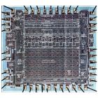
1971 – 将微处理器的功能集成到一个 CPU 芯片上 硅栅 加工与成型技术的产生使得计算机中央处理器 (CPU) 压缩到一块单独的芯片上 在二十世纪六十年代末,设计人员致力于把计算机中央处理器的功能集合到微小的 MOS 大规模集成电路芯片上,这种技术被称为微处理器单元 ( 单片机 ) 芯片集合。 1969 年 Lee Boysel 创造了 Four-Phase 系统有限公司,他在一块半导体上设计植入了早期的八位逻辑算术单元(设计 3800/3804 型)。一个 8 位的 AL-1CPU 片被扩展到了 32 位。在 1970 年 , Garrett AiResearch 的 Steve Geller 和 Ray Holt 设计的 MP944 芯片被用于 F-14A 中央大气数据计算机的芯片,它是被 AMI 公司由六个金属栅晶片组成的。 英特尔的第一个微处理器—— 4004 ,来源于 Ted Hoff 和 Stanley Mazor 的构想。得益于 Masatoshi Shima ,在 1971 年, Federico Faggin 根据 Shima 在硅栅 MOS 芯片技术( 1968 年里程碑式的发展)的经验,将一个由 2300 个晶体管组成的四位微处理器放入到 16-pin 封装起来。 Faggin 指导 Hal Feeney 设计的 8 位 8008 设备于 1972 年公布。为 CTC 公司(即后来的 Datapoint 公司)设计的 8008 设备的原型也曾被德州仪器用于 TMX1795 系统,但是却从没有被用于商业用途。第二代 8 位的设计来源于 Intel ( 设计 8080 型 ) 和 Tom Bennett 在 Motorola 领导的一个团队(设计 6800 型), Tom Bennett 在 1974 年建立被广泛接受的微处理器理念。从 MOS 集成电路技术 -6502 体系衍生出的廉价变种 6800 使得个人电脑和来自于 Apple, Atari, Commodore 或其他公司的游戏可以任意连接。在二十世纪七十年代中期,许多供应商提供增强的 8 位结构,其中 Zilog 公司的最为强大。两个 1975 微处理器预示着后来重要发展趋势,包括在 IBM 工作过的 RCA 的 CMOS COSMAC(1802 里程碑 ) 与 John Cocke 801 精简指令集。 译者:哈尔滨工业大学(威海)电子封装 090840221-马东超 校对: http://www.computerhistory.org/semiconductor/timeline/1971-MPU.html 版权 copyright by www.computerhistory.org 1971 - Microprocessor Integrates CPU Function onto a Single Chip Silicon-gate process technology and design advances squeeze computer central processing units (CPU) onto single chips. By the late -1960s, designers were striving to integrate the central processing unit (CPU) functions of a computer onto a handful of MOS LSI chips, called microprocessor unit (MPU) chip sets. Building on 8-bit arithmetic logic units (3800/3804) he designed earlier at Fairchild , in 1969 Lee Boysel created the Four-Phase Systems Inc. AL-1 an 8-bit CPU slice that was expandable to 32-bits. In 1970 Steve Geller and Ray Holt of Garrett AiResearch designed the MP944 chip set to implement the F-14A Central Air Data Computer on six metal-gate chips fabricated by AMI. Intel's first microprocessor, the 4004, was conceived by Ted Hoff and Stanley Mazor. Assisted by Masatoshi Shima , Federico Faggin used his experience in silicon-gate MOS technology ( 1968 Milestone ) to squeeze the 2300 transistors of the 4-bit MPU into a 16-pin package in 1971. Faggin also supervised Hal Feeney 's design of the 8-bit 8008 device announced in 1972. Designed for CTC ( later Datapoint ), prototypes of the 8008 function were also built by Texas Instruments as the TMX1795 but never offered commercially. Second generation 8-bit designs from Intel (8080) and from a team led by Tom Bennett at Motorola (6800) in 1974 established widespread acceptance of the MPU concept. A low-cost variant on the 6800 architecture by MOS Technology (6502) enabled personal computers and games from Apple, Atari, Commodore and others. By the mid-1970s many vendors offered enhanced 8-bit architectures, with Zilog 's Z80 being the most enduring. Two 1975 MPUs that presaged important later trends included RCA's CMOS COSMAC 1802 (1963 Milestone ) and John Cocke ’s 801 RISC device at IBM. Beginning in the mid-1970s, 16-bit MPUs emerged from General Instrument (CP1600), National (PACE), TI (TMS9900), and Zilog (Z8000). Boosted by the PC boom of the 1980s, Intel's 8086/8088 (IBM PC) and Motorola's 68000 (Macintosh) devices enjoyed the widest market success. 四相系统,Inc。AL-1 8位计算机处理器片。1968年十月设计开始。1969年三月配置设备。 金色的内连线突出了Intel 4004微处理器复杂的内部构局 2007年5月,Intel 4004开发团队合影T. Hoff, H. Feeney, S. Mazor, M. Shima, F. Faggin Busicom 计算机的MCS-4内部图片,设置有4004微处理器
IBM的工程师们开发了用以减少研发错误和设计时间的计算机辅助电子设计自动化工具。 当集成电路开始包含几百个门电路和数以千计的晶体管时,他们所支持的计算机已经可以完成加快设计速度和减少设计错误的任务了。这个方法被称作 CAD (计算机辅助设计)或者 EDA (电子设计自动化)。 IBM 在 20 世纪 50 年代末率先开发了在 700 系列电脑文档下运行的 EDA 程序。到了 1966 年, James Koford 和他的同事们在 IBM 纽约州东费西基尔公司用图形显示器采集 STL 混合电路模块( 1964 里程碑事件)的图案,检查他们的错误并自动将信息转换为掩膜模式。在 Koford 加入 Fairchild RD 后他又与 Hugh Mays 、 Ed Jones 及其他同事一起将这项程序应用于单片集成电路。他们的努力创造了逻辑模拟软件( FAIRSIM )、测试程序生成器软件以及门列阵和标准单元布局布线软件( 1967 年里程碑事件),这些为一代又一代的 EDA 工具打下了坚实的基础。 EDA 有两个重要项目源于非主流产业。 20 世纪 60 年代, Larry Nagel 和 Donald Pederson 以及后来的贡献者 Richard Newton 在美国加州大学伯克利分校开发了 SPICE (模拟集成电路重点项目)电路仿真程序。 1979 年,加州理工学院的 Lynn Conway of Xerox 和 Carver Mead 在他们论著的《超大规模集成电路系统导论》中描述的一个新方法揭开了系统设计和芯片设计过程秘密。 20 世纪 80 年代,益华电脑和美国新思科技公司受到在柏克莱加州大学( SIS )、洛杉矶加利福尼亚大学( RSAP )和科罗拉多大学( BOLD )所做调查的激发,开始对综合逻辑系统进行商业化的包装。这些和先进的布局布线技术、逻辑模拟技术以及其他厂商已有的设计核查规则共同使集成电路的设计生产能力能够紧跟设备复杂度不断增加的步伐。 IBM 360/67 仙童公司 1967 年的以大型计算机为运算动力的 CAD 设计系统 图 1 编辑者:费尔柴尔德摄像机仪器公司 掩模草图数字化手绘系统工具 图 2 提供者:因特尔公司 20 世纪 80 年代基于集成电路 CAD 设计系统的工作站 图 3 米德和加威的成就获得了 1981 年的美国电子奖 图 4 译者:哈尔滨工业大学(威海)电子封装 090840213- 邱东阳 校对:哈尔滨工业大学(威海)电子封装 090840229-朱泯西 版权 copyright by www.computerhistory.org 1966 - Computer Aided Design Tools Developed for ICs IBM engineers pioneer computer-aided electronic design automation tools for reducing errors and speeding design time. IBM 360/67 mainframe-powered CAD system at Fairchild in 1967 Credit: Fairchild Camera Instrument Corporation Mask layout drawing hand digitizing system tool Courtesy of: Intel Corporation Workstation-based integrated circuit CAD system 1980s 1981 Electronics Award for Achievement to Conway and Mead As ICs began to incorporate hundreds of gates and thousands of transistors, the computers they enabled were harnessed to speed the design task and eliminate errors. This process is called CAD (Computer Aided Design) or EDA (Electronic Design Automation). IBM pioneered EDA in the late 1950s with documentation of the 700 series computers. By 1966 James Koford and his colleagues at IBM Fishkill were capturing SLT hybrid circuit module ( 1964 Milestone ) designs on graphical displays, checking them for errors and automatically converting the information into mask patterns. After Koford joined Fairchild RD he worked with Hugh Mays, Ed Jones, and others to apply this process to monolithic ICs. Their efforts created logic simulators (FAIRSIM), test program generators, and place and route software for gate arrays and standard cells ( 1967 Milestone ) that laid the ground work for generations of EDA tools. Two important EDA projects originated outside the mainstream of the industry. Larry Nagel and Donald Pederson, with later contributions by Richard Newton, at U.C. Berkeley developed the SPICE (Simulation Program with IC Emphasis) circuit simulation program in the 1960s. A new methodology described in the 1979 Introduction to VLSI Systems by Lynn Conway of Xerox, PARC and Carver Mead of California Institute of Technology demystified the process of chip design for system designers. Commercial logic synthesis packages from Cadence and Synopsys in the 1980s were stimulated by research at U.C. Berkeley (SIS), U.C.L.A. (RASP), and University of Colorado, Boulder (BOLD). These, together with advancements in place and route, logic simulation, and design rule verification from other vendors, allowed IC design productivity to keep pace with increasing device complexity.
第三方供应商发展到具备了半导体结构的专业知识,并且作为技术改进的及关键部分生产设备的供应商出现。 在半导体工业发展的第一个十年,行业推行了 5 种基本结构的晶体管:点接触式晶体管、生长结式晶体管、合金结式晶体管、表面势垒式晶体管和扩散底层式晶体管。 制造商架构起他们自己的生产设施设备投入到每一代产品的制造中。杰克 ·基尔比( 1958 年里程碑式人物)注意到说:“可能我们用到的设备的最贵的那一部分要花费至少 1 万美金 。 由于产品通过平面法( 1959 年的里程碑)向大型化发展,因此出现了产业的和独立的设备制造商,从而将工艺技术也标准化了。制造商专门研究了前端(晶圆加工)和后端(封装、组配和测试)( 1961 年的里程碑)的生产运行。 前端的生产设备,随着晶圆尺寸从 1958 年的 0.5 英寸增大到今天的 12 英寸( 300mm ),其价格也呈数量级增长。早期的前端的生产设备配套供应商包括赛默公司(扩散熔炉)和它旗下的日本电子有限公司、 DW 工业(沉积系统),以及 GCA Mann 和铂金埃尔默公司(光刻设备)( 1955 年的里程碑)。伊智公司, 1961 年费雅嘉分拆出的一个子公司,生产建造了用于晶圆测试的探测设备。 瓦里安公司建造了蒸发器、真空泵和离子注入系统。成立于 1967 年,为制造外延薄膜( 1960 年的里程碑)提供化学气相沉积系统的应用材料公司,通过鼓励半导体供应商将其对制造工艺开发发展工作转交给他们的设备供应商,从而给行业动向带来了改变。 技术工艺的第三方资源,使半导体公司得以关注产品的体系结构及应用,而不再关注于生产和制造工艺的专业知识。这就造成了晶圆代工工厂的兴起,在 19 世纪 80 年代,这些工厂支持了作为新类型的无晶半导体公司的发展。 译者:哈尔滨工业大学(威海)电子封装 090840214葛峰 校对:哈尔滨工业大学(威海)电子封装 090840215申聪敏 原文: http://www.computerhistory.org/semiconductor/timeline/1967-Equipment.html 版权 copyright by www.computerhistory.org 1967 - Turnkey Equipment Suppliers Change Industry Dynamics Third-party vendors develop specialized knowledge of semiconductor fabrication and emerge as vendors of process technology and turnkey manufacturing facilities. During its first decade the semiconductor industry went through five basic transistor structures: point contact, grown junction, alloyed junction, surface barrier, and diffused-base. Manufacturers built their own equipment to support each generation. Jack Kilby ( 1958 Milestone ) noted that "probably the most expensive piece of equipment that we used cost less than $10,000." As production moved to high volumes with the planar process ( 1959 Milestone ), techniques were standardized across the industry and independent equipment producers emerged. Vendors specialized in "Front End" (wafer processing) or “Back End” (package, assembly, and test) ( 1961 Milestone ) operations. Front-end equipment prices increased by orders of magnitude as wafer diameters grew from 0.5 inches in 1958 to today’s 12 inches (300mm). Early front-end tool suppliers include Thermco (diffusion furnaces) and its Japanese licensee Tokyo Electron Ltd, DW Industries (deposition systems), and GCA/Mann and Perkin Elmer (photolithography) ( 1955 Milestone ).Electroglas, a 1961 Fairchild spinout, built probe equipment for wafer testing. In 1965 Kulicke Soffa introduced commercial contact aligners. Varian Associates built evaporators, vacuum pumps, and ion-implantation systems. Founded in 1967 to supply chemical vapor deposition systems for epitaxial films ( 1960 Milestone ), Applied Materials initiated a change in industry dynamics by encouraging semiconductor vendors to shift responsibility for development of manufacturing technology to their equipment suppliers.Third-party sources of technology allowed the semiconductor companies to focus on product architecture and applications rather than process and manufacturing expertise. This led to the rise of "wafer-foundry" vendors who supported a new breed of "fabless" semiconductor companies in the 1980. Michael McNeilly Walter Benzing pioneered epitaxial deposition equipment at Applied Materials, Inc. (应用材料公司倡导外延沉积设备的先驱——迈克尔 ·麦克尼尔,沃尔特·本辛 ) Credit : Semiconductor Equipment and Materials International (SEMI) Applied Materials Model AMV 800 chemical vapor deposition epitaxial reactor (1969) (应用材料公司化学气相沉积外延反应设备 AMV 800 模型) Credit : Applied Materials Technology, Inc Electroglas Model 131B Motorized/Manual Prober allowed testing of die on the wafer before packaging (伊智公司的用于测试封装前晶圆上芯片的自动 / 手动探测器 131B 模型) Credit : Electroglas, Inc Perkin Elmer Micralign projection mask aligner team 1973 ( 1973 年铂金埃尔默公司的 Micralign 投射掩膜对准器团队) Credit : Semiconductor Equipment and Materials International (SEMI)
1956- 硅片在硅谷首次出现 肖克利半导体实验室 建造了 加州北部的第一个原型开发半导体设备 来为 硅谷训练年轻的工程师和科学家 。 1955 年 9 月 , 威廉萧克利和阿诺贝克曼同意 建立肖克利半导体实验室作为贝克曼的部门来“积极 、大力开展 关于半导体材料的 活动 ”。肖克利在加利福尼亚州山景城 圣安东尼奥南部道路 租用了 391 号楼,同时,开始招聘“世界上 最有创造力的团队开发、设计、生产晶体管 ”。 他吸引了很 多 能干的工程师和科学家 ,其中 了解和开发硅相关技术和工艺 、 扩散 技术的 戈登 · 摩尔和罗伯特 · 伊斯 都被他招聘来工作。 1956 年 12 月萧克利 因为 发明晶体管获得了诺贝尔物理学奖 ,但是,他的助理开始厌倦了他懒散的管理模式。 他们也觉得公司应该追求更直接生产硅晶体管的机会 而不是期盼遥远的目标“他在实验室将硅应用到电话通讯领域”。 在要求肖克利再雇用一名新的管理后, 摩尔 、 尤利乌斯 · 伊斯 、 格里尼克 、 琼 · 霍尔尼 、 克莱纳 、 拉斯特 、 罗伯茨 8 名 萧克利员工 在 1957 年 9 月 辞职并创立了 美国飞兆半导体公司 在 帕洛阿尔托 。 许多 来自 播实之星的员工 随之而来。 在未来十年 里, 快捷半导体 成长为 在半导体产业最重要的和创新的公司 ,引导了硅谷其他企业科技和文化,其中超微半导体和 英特尔 连接技术,但是,他的公司从来没有获得实际的利润。 贝克曼 在 1960 年 把专利卖给了 Clevite 公司 。 萧克利在斯坦福大学成了一个教授的电气工程与应用科学 的老师。 Toasting Shockley's Nobel Prize award at Rickey's Hotel, Palo Alto, CA. Celebrants include G. Moore, S. Roberts, R. Noyce, and J. Last 肖克利诺贝尔奖奖在里奇的酒店,帕洛阿尔托约礼,包括穆尔,罗伯茨,诺伊斯,和 J · The Shockley Semiconductor Laboratory facility, Mountain View, CA. circa 1960. 肖克利半导体实验室设施,山景,约公元 1960 。 Small-scale silicon zone refining in the Shockley laboratory in Mountain View 小型硅精炼的肖克利实验室在山景 Small-scale silicon zone refining in the Shockley laboratory in Mountain View 小型硅精炼的肖克利实验室在山景 1956 - Silicon Comes to Silicon Valley Shockley Semiconductor Laboratory develops Northern California's first prototype silicon devices while training young engineers and scientists for the future Silicon Valley. In September 1955 William Shockley and Arnold Beckman agreed to found the Shockley Semiconductor Laboratory as a Division of Beckman Instruments "to engage promptly and vigorously in activities related to semiconductors." Shockley rented a building at 391 South San Antonio Road in Mountain View, California, and began recruiting "the most creative team in the world for developing and producing transistors." He attracted extremely capable engineers and scientists, including Gordon Moore and Robert Noyce, who learned about and developed technologies and processes related to silicon and diffusion while working there. In December 1956 Shockley shared the Nobel Prize in Physics for inventing the transistor, but his staff was becoming disenchanted with his difficult management style. They also felt the company should pursue more immediate opportunities for producing silicon transistors rather than the distant promise of a challenging four-layer p-n-p-n diode he had conceived at Bell Labs for telephone switching applications. After unsuccessfully asking Beckman to hire a new manager, eight Shockley employees - including Moore and Noyce plus Julius Blank, Victor Grinich, Jean Hoerni, Eugene Kleiner, Jay Last and Sheldon Roberts - resigned in September 1957 and founded the Fairchild Semiconductor Corporation in Palo Alto. Many other employees, from technicians to PhDs, soon followed. Over the next decade, Fairchild grew into of the most important and innovative companies in the semiconductor industry, laying the technological and cultural foundations of Silicon Valley while spinning off dozens of new high-tech start-ups, including Advanced Micro Devices (AMD) and Intel. Shockley continued pursuing his four-layer diode but his company never realized a profit. Beckman sold the operation to Clevite Corporation in 1960. Shockley became a professor of electrical engineering and applied science at Stanford University. 译者:哈尔滨工业大学(威海)电子封装 090840120-王开伟 校对:哈尔滨工业大学(威海)电子封装 090840117-康志龙
在十九世纪五十年代,半导体设备在数字计算机上逐渐取代了真空管。直到十九世纪六十年代新设备完全晶体管化。 1950年4月,国家统计局的计算机开始工作,它使用了10,500个锗二极管和747个真空管。 在曼彻斯特大学托姆 基尔伯恩 教授手下学习,瑞查德 格瑞斯达尔和道格拉斯韦伯,于1953年11月16号展示了一台晶体管计算机的原型。这台由 卫星试验中心 制造的 48位的机器用了92个点相连的晶体管和550个二极管,装备到 美国埃梯梯 的联合王国的长途电话中继线装备。一代拥有 250个晶体管结 加强版于 1955年完成。MV电子公司制造了具有六个单元结构,同样拥有该结构 Metrovick950已从 1956年在公司内部实行商业推广。 在1954年,JEANH.FELKER领导一个包括工程师JAMES.R.HARRIS的来自贝尔实验室的研究小组为美国空军设计制造了一台全晶体管计算机,称之为TRADIC(晶体管电子计算机),该机包括大约700个 点接触晶体管和10000个二极管。当该试验机型工作在1MHZ的频率下时,功耗仅不到100W。一个更轻的机载版本(飞行版TRADIC)使用了结形晶体管取代了在C-131飞机上用于导航和控制航弹空投的模拟计算机。由WILLIAMPAPIAN领导的来自麻省理工学院林肯实验室的先进技术发展小组的成员在1956年4月使用来自PHILCO公司的高速锗开关晶体管搭建了速度达5MHZ的通用计算机,也就是众所周知的TX-0(晶体管实验性型)。同样在1956年,日本的第一台通用计算机,ETL3型,使用了130个点接触晶体管和1800个二极管。这台机器是由位于东京的电子技术实验室的HiroshiWada领导研发的. The SEAC computer operator's station 图一:东部标准自动计算机操作员的工作台 University of Manchester (UK) "Manchester TC" transistor computer 图二:联合王国曼彻斯特大学“曼彻斯特TC”晶体管计算机 J. H. Felker and J. R. Harris work on the Bell Labs TRADIC computer 图三:JH菲尔克和JR哈瑞斯在贝尔实验室的TRDIC计算机前工作 The RCA 501 computer, one of the first commercial transistorized machines in the U.S., was announced in 1958 图四:RCA 501计算机,美国第一台商业晶体管计算机在1958年面世 译者:哈尔滨工业大学(威海)电子封装 090840115-刘金鑫 校对:哈尔滨工业大学(威海)电子封装 090840116-赵英建 原文 http://www.computerhistory.org/semiconductor/timeline/1953-transistorized-computers-emerge.html 版权 copyright by www.computerhistory.org ———————————————————————————————— 1953 - Transistorized Computers Emerge During the 1950s, semiconductor devices gradually replaced vacuum tubes in digital computers. By 1960 new designs were fully transistorized. Operational in April 1950, the National Bureau of Standards Eastern Automatic Computer (SEAC) employed 10,500 germanium diodes and 747 vacuum tubes. Working under Tom Kilburn at Manchester University, Richard Grimsdale and Douglas Webb, demonstrated a prototype transistorized computer on November 16, 1953. The 48-bit machine used 92 point-contact transistors and 550 diodes fabricated by STC, the UK arm of ITT. An enhanced version with 250 junction transistors was completed in 1955. The Metropolitan Vickers Electrical Company manufactured six units as the Metrovick 950, which they used commercially within the company from 1956. Jean H. Felker led a Bell Labs team including engineer James R. Harris that designed and built a fully transistorized computer dubbed TRADIC (TRAnsistor DIgital Computer) for the U. S. Air Force in 1954. Involving about 700 point-contact transistors and over 10,000 diodes, the prototype operated at 1 MHz while requiring less than 100 watts of power. A lighter airborne version (Flyable TRADIC) using junction transistors replaced an analog computer for navigation and bombing control in a C-131 aircraft. Led by William Papian, in April 1956 members of the Advanced Development Group of MIT Lincoln Labs used fast germanium switching transistors from Philco Corporation to build a 5 MHz general-purpose digital computer known as TX-0 (Transistor Experimental). Also in 1956, Japan’s first transistorized computer, the ETL Mark III, using 130 point-contact transistors and 1800 diodes was built under the direction of Hiroshi Wada at the Electrotechnical Laboratory in Tokyo.
1958年 - 所有半导体固态电路得以证明 杰克.基尔比用半导体材料制造了一个兼有主动与被动部分的微型电路。 随着计算机系统变得更加复杂,工程师们也在寻求更加简单的方法去连接他们所使用的数以万计的晶体管。政府机构资助微型模块和多芯片混合电路工程来解决这个问题。 1952 年,英国电信研究机构的 GWA Dummer 提出“随着晶体管的问世和半导体领域的广泛研究,现在看来可以设想出一种没有连接线的电子设备,并使之封闭于一个固体块中。” 从 50 年代中期到后期,一系列的项目成功地将多个组件集成于一个芯片上。在美国无线电公司, Harwick Johnson 取得了一个无线电振荡器专利, Torkel Wallmark 和 Sanford Marcus 分别创立了移位寄存器和逻辑门。 阿瑟 · 德阿萨罗和伊恩 · 罗斯贝尔实验室制作出了电话应用方面的四阶段计数器。 IBM 公司的乔 · 罗格和里克 · 迪尔制作出了一台使用双基极二极管结构的电脑。日本通产省的 Yasuro Tarui 和德州仪器的 Richard Stewart 提交了多个设备专利。 麻省理工学院的 Dudley Buck 研发了一种超导集成元件制成的低温管。尽管这些成就取得了不同程度的功能,但是没有一个可以解决通用性的系统集成带来的挑战。 1958 年 9 月 12 日,来自德州仪器的 Jack Kilby 在锗基片上用 PNP 型晶体管自己刻蚀制作了一个含有晶体管、电阻、电容等原件的电路。通过使用精致的金制“神奇导线”,他将各自分立的原件连接到了一个振荡电路。一个星期之后,他制作出了放大器。德州仪器在 1959 年 3 月宣布了 Kilby 的“固体电路”概念,并在 1960 年 3 月推出其首个商业设备, 502 型号的二进制触发器,每个售价为 450 美元。但是金线互联并不是一个实用的生产技术。 1961 年 10 月,德州仪器推出的 51 系列直接藕合晶体管逻辑 “ 完全集成电路 ” 系统,使用敷金属平面技术( 1959 年里程碑) 。 图一: Jack Kilby with his lab notebook open at his first solid circuit drawing 杰克 · 基尔比与他的实验室笔记本,展示了他的第一固体电路图纸 Courtesy of: Texas Instruments, Inc 图二: Kilby’s original germanium multi-chip "solid-circuit" oscillator Kilby 的原锗多芯片 “ 固体电路 ” 振荡器 Courtesy of: Texas Instruments, Inc 图三: Connection diagram and open package photograph of the Type 502 flip-flop with "flying-wire" internal connections 连接图和 502 型 “ 飞线 ” 的封装内部连接触发器 Courtesy of: Texas Instruments, Inc 图四: G.W.A. Dummer predicted "solid block" circuits in 1952 G.W.A. dummer 1952 年预测 “ 固体块 ” 电路 Credit: Robert Cathles, under GNU Free Documentation License 译者:哈尔滨工业大学(威海)电子封装 090840123-薛彦峰 校对:哈尔滨工业大学(威海)电子封装 090840125-赵宏博 原文: http://www.computerhistory.org/semiconductor/timeline/1958-Miniaturized.html 版权 copyright by www.computerhistory.org 原文: 1958 - All semiconductor "Solid Circuit" is demonstrated Jack Kilby produces a microcircuit with both active and passive components fabricated from semiconductor material. As computer systems grew more complex, engineers sought simpler ways to interconnect the thousands of transistors they employed. Government agencies funded micro-module and multi-chip hybrid circuit projects in search of a solution to this problem. In 1952, G. W. A. Dummer of England's Telecommunications Research Establishment proposed "With the advent of the transistor and the work in semiconductors generally, it seems now possible to envisage electronic equipment in a solid block with no connecting wires." From the mid to late 1950s several projects succeeded in integrating multiple components on a chip. At RCA Harwick Johnson patented an oscillator and Torkel Wallmark and Sanford Marcus built shift registers and logic gates. Arthur D'Asaro and Ian Ross of Bell Labs fabricated a four-stage counter for telephone applications. Joe Logue and Rick Dill of IBM built a counter using a double-base diode structure. Yasuro Tarui of Japan's MITI and Richard Stewart of TI filed multiple device patents. Dudley Buck of MIT developed the cryotron, an integrated superconducting element. While achieving various degrees of functionality, none of these ideas yielded a solution to the challenge of general-purpose system integration. On September 12, 1958, Jack Kilby of Texas Instruments built a circuit using germanium mesa p-n-p transistor slices he had etched to form transistor, capacitor, and resistor elements. Using fine gold "flying-wires" he connected the separate elements into an oscillator circuit. One week later he demonstrated an amplifier. T.I. announced Kilby's "solid circuit" concept in March 1959 and introduced its first commercial device in March 1960, the Type 502 Binary Flip-Flop priced at $450 each. However the flying-wire interconnections were not a practical production technique. In October 1961, T.I. introduced the Series 51 DCTL "fully-integrated circuit" family using deposited-metal planar technology ( 1959 Milestone ).
1959 年 “ 平面 ” 制造工艺的发明 Jean Hoerni 发展平面工艺解决了晶体管可靠性问题 , 从而使半导体制造革命化。 与台面晶体管( 1958 里程碑)的可靠性问题寻求解决方案, Fairchild 的物理学家 Jean Hoerni 回忆起他曾在 1957 年 12 月记录的想法 — 一个新的进程,在离开氧化层的硅片上,以保护敏感的 PN 下面的路口。由于专注于首批设备的投入生产,在那时该公司没有追求这种做法。 由于担心可能的污染物,传统的智慧,也需要去除氧化物掩蔽完成后这一层,从而暴露了路口。 Hoerni 观看氧化物,而不是作为一种可能的解决方案 - 他的“平面”的方法,成品设备的地势平坦而命名,会保护这些路口。在 1959 年 1 月编写了专利披露后,那年三月,他证明了工作平面晶体管的存在。就像霍尔尼曾预言过的,确实发现氧化层保护的路口。 平面器件也被证明有更好的电气特性 - 尤其是远低漏电流,这是计算机逻辑设计中的关键。他们允许从一个晶圆( 1960 里程碑)侧面制造集成电路的所有组件。 1960年4月,仙童公司推出了商业性的2N1613平面晶体管,并注册了该工艺在工艺中的所有权。今天的 10 亿个晶体管的集成电路全部依靠的是 Hoerni 的突破性理念。一位历史学家称它是“在半导体产业史上最重要的创新。” 虽然平面技术使硅晶体管以满足航空航天工业的严格要求,但是半导体厂商在遇到的每一个重大的技术进步的同时也会遇到新的麻烦。在 20 世纪 60 年代的重大问题,包括金丝上的“紫色的瘟疫”,铝与电的连线,和 MOS 晶体管的稳定。 1964 年(里程碑) 图一: 1 Jean Hoerni with transistor geometry in the background Jean Hoerni 在晶体管几何背景下的的照片 图二: Photomicrograph of a Model 2N1613 planar transistor 2N1613 平面晶体管模型的照片 图三: Figure from Hoerni’s patent on the planar manufacturing process Hoerni 的从图上显示的平面制造工艺过程的照片 图四: Cutaway view of an early Fairchild planar transistor 早期 Fairchild 平面晶体管的剖视图 译者:哈尔滨工业大学(威海)电子封装 090840124-于凯先 校对: 原文: http://www.computerhistory.org/semiconductor/timeline/1959-invention-of-the-planar-manufacturing-process-24.html 版权 copyright by www.computerhistory.org 原文: 1959 - Invention of the "Planar" Manufacturing Process Jean Hoerni develops the planar process to solve reliability problems of the mesa transistor, thereby revolutionizing semiconductor manufacturing. Seeking a solution to reliability issues with the mesa transistor ( 1958 Milestone ), Fairchild physicist Jean Hoerni recalled an idea he had recorded in December 1957 - a new process in which the oxide layer is left in place on the silicon wafer to protect the sensitive p-n junctions underneath. Focused on getting its first devices into production, the company did not pursue the approach at that time. Due to concerns about possible contaminants, conventional wisdom required removing this layer after completion of oxide masking, thus exposing the junctions. Hoerni viewed the oxide instead as a possible solution - his "planar" approach, named after the flat topography of the finished device, would protect these junctions. After writing a patent disclosure in January 1959, he demonstrated a working planar transistor that March. The oxide layer was indeed found to protect the junctions, as Hoerni had predicted. Planar devices also proved to have better electrical characteristics - particularly far lower leakage currents, which is critical in computer logic design. And they permitted fabrication of all the components of an integrated circuit from one side of a wafer ( 1960 Milestone ). Fairchild introduced the 2N1613 planar transistor commercially in April 1960 and licensed rights to the process across the industry. The billion-transistor integrated circuits of today rely on Hoerni’s breakthrough idea. One historian has called it "the most important innovation in the history of the semiconductor industry." While planar technology enabled silicon transistors to meet the stringent demands of the aerospace industry, semiconductor vendors continued to encounter new failure mechanisms with every major technology advance. Significant issues in the 1960s included “purple plague” on gold bonding wires, electromigration of aluminum interconnect lines, and MOS transistor stability. ( 1964 Milestone )
1960-第一个平面集成电路的制作 Jay Last引领了基于Hoerni的平面法和Noyce的整体方法的第一个商用IC的发展。 1959年8月Fairchild半导体研发主任Robert Noyce让共同创立者Jay Last开始开发一个基于Hoerni的平面法(1959里程碑)和Noyce的专利(1959里程碑)的平面集成电路。在Wescon用分立晶体管建立了一个多芯片触发器来诠释概念之后,Last组成了一个包括Sam Fok, Isy Haas, Lionel Kattner, 和 James Nall的团队。根据应用部门的Don Farina, Robert Norman提供的特性化数据,用一个改良的直接耦合晶体管逻辑(DCTL)电路设计了一个带有4晶体管和5个电阻器的兼有早期平面处理能力集成电路。 在一个芯片上集成多重相连的装置造成了许多新的工程挑战。1960年5月26日生产的第一个工作的单块集成电路设备使用了物理隔离来实现组件之间的电隔离。硅晶圆的背面刻蚀了深凹槽并且充满了不导电的环氧树脂。由Haas and Kattner研发的用硼扩散技术来实现p-n节电子隔离成为了首选的生产方法,并在1960年9月27日投入了集成电路的生产。 1960年Fairchild在工程会议提出了先进的信息并提供了面向的客户原型样品。在名为Logic (Micrologic)的贸易下,”F” 类型触发器功能在1961年通过一个在纽约的新闻发布会上展示广告和《生活》杂志上的一张照片向社会公告。五个包括" G "类型门功能(1962里程碑),半加法器和一个半移位寄存器的外加的电路在10月被应用。 Jay Last with Gordon Moore in background Jay Last和Gordon Moore在背景下 Credit: Fairchild Camera Instrument Corporation Physically-isolated Micrologic flip-flop compared to a dime from LIFE magazine March 10, 1961 物理隔离的微程序控制逻辑触发器与硬币相比,摘自1961年3月10日的生活杂志 Credit: Fritz Goro, Time Life Pictures Junction-isolated version of the type "F" flip-flop. The die were etched to fit into a round TO-18 transistor package 节孤立版本的“F”类型触发器。晶片被蚀刻来适应一个圆TO-18晶体管封装。 Credit: Fairchild Camera Instrument Corporation Presentation block with a Micrologic wafer and IC in the TO-18 package 一个微程序控制逻辑晶圆和集成电路在圆TO-18晶体管封装中的展示块 CHM collection: Gift of Bob and Marcella Major 译者:哈尔滨工业大学(威海)电子封装 090840126-种兆永 校对:哈尔滨工业大学(威海)电子封装 090840124-于凯先 原文 http://www.computerhistory.org/semiconductor/timeline/1960-FirstIC.html 版权 copyright by www.computerhistory.org ———————————————————————————————————— 1960 - First Planar Integrated Circuit is Fabricate Jay Last leads development of the first commercial IC based on Hoerni’s planar process and Noyce’s monolithic approach. In August 1959 Fairchild Semiconductor Director of RD, Robert Noyce asked co-founder Jay Last to begin development of an integrated circuit based on Hoerni’s planar process ( 1959 Milestone ) and Noyce’s patent. ( 1959 Milestone ) After building a multi-chip flip-flop with discrete transistors to demonstrate the concept at Wescon, Last assembled a team including Sam Fok, Isy Haas, Lionel Kattner, and James Nall. Based on characterization data prepared by Don Farina, Robert Norman of the applications department designed a flip-flop with four-transistors and five resistors using a modified Direct Coupled Transistor Logic (DCTL) circuit as most compatible with early planar processing capabilities. Integrating multiple interconnected devices on one chip posed many new engineering challenges. The first working monolithic devices produced on May 26 1960 used physical isolation to achieve electrical separation between components. Deep channels were etched from the rear of the silicon wafer and filled with non-conducting epoxy. The preferred production method, p-n junction electrical isolation using a boron diffusion technique developed by Haas and Kattner, yielded working circuits on September 27, 1960. Fairchild presented advanced information at engineering conferences and provided prototype samples to customers in 1960. Under the trade name Logic (Micrologic), the type "F" flip-flop function was announced to the public in March 1961 via a press conference at the IRE Show in New York and a photograph in LIFE magazine. Five additional circuits, including the type "G" gate function ( 1962 Milestone ), a half adder, and a half shift register, were introduced in October.
图1 Dawon Kahang的金属氧化物半导体(mos)晶体管的图形 M. M. (John) Atalla and Dawon Kahn g 在 1995 年于贝尔实验室成功制造了第一个绝缘栅极场效应晶体管,一直被 Lilienfeld, Heil, Shockley 等人长期期望的通过注入到半导体材料来克服表面态从而封锁电场。通过研究二氧化硅热生长层,他们发现这些 ** 会在一个由金属(金属极),氧化物(氧绝缘层),硅(硅半导体)组成的三明治(也就是 金属氧化物半导体场效应晶体管,通常被成为金属氧化物半导体 )的硅及其氧化物之间有一个明显的减小。因为他们的装置缓慢而起在电话系统中没有很急切的需求,所以它没有进一步的发展。在一个 1961 年的备忘中, Kahng 却指出了它在易于制造和在集成电路方面应用的可能性的潜力,飞兆半导体和美国无线电公司的研究人员认识到了这些优势。在 1960 年 Karl Zaininger 和 Charles Meuller 在美国无线电公司制造了一个 金属氧化物半导体晶体管,飞兆半导体的 C.T. Sah 制造了一个可控金属氧化物半导体四极管。 Fred Heiman and Steven Hofstein 随后在美国无线电公司于 1962 年研制出了 实验用 16 个晶体管的集成装置。 图2仙童半导体的FI 100 的p沟道金属氧化物半导体开关晶体管 金属氧化物半导体晶体管的导电区域要么是 p 型 ( 称其 p 沟道 设备 ) 或 n 型 (n- 沟道设备 ) 材料,后者要比 p 沟道的更快,同时也更难制作。 金属氧化物半导体器件 在 1964 年冲击了商业市场。通用微电子公司和飞兆半导体公司将 p 型装置用于逻辑开关。美国无线电公司引进了一种 n 沟道的晶体管用于放大信号。由于它比双极性器件有更小的尺寸和功率消耗,如今超过百分之 99 的微型芯片都用金属氧化物半导体器件来制作。取得这样的普遍应用耗费了十年努力。 图3 RCA16金属半导体晶体管的电路放大图像 图4 1962年在RCA的 MOS IC开发者 Steven Hofstein 译者:哈尔滨工业大学(威海)电子封装 090840127-周超 校对:哈尔滨工业大学(威海)电子封装 090840128- 徐涛 原文 http://www.computerhistory.org/semiconductor/timeline/1978-PAL.html 版权 copyright by www.computerhistory.org ———————————————————————————————— 1960 - Metal Oxide Semiconductor (MOS) Transistor Demonstrated John Atalla and Dawon Kahng fabricate working transistors and demonstrate the first successful MOS field-effect amplifier. In 1959 M. M. (John) Atalla and Dawon Kahng at Bell Labs achieved the first successful insulated-gate field-effect transistor (FET), which had been long anticipated by Lilienfeld, Heil, Shockley and others ( 1926 Milestone ) by overcoming the surface states that blocked electric fields from penetrating into the semiconductor material. Investigating thermally grown silicon-dioxide layers, they found these states could be markedly reduced at the interface between the silicon and its oxide in a sandwich comprising layers of metal (M - gate), oxide (O - insulation), and silicon (S – semiconductor) - thus the name MOSFET, popularly known as MOS. As their device was slow and addressed no pressing needs of the telephone system, it was not pursued further. In a 1961 memo, however, Kahng pointed out its potential ease of fabrication and the possibility of application in integrated circuits. But researchers at Fairchild and RCA did recognize these advantages. In 1960 Karl Zaininger and Charles Meuller fabricated an MOS transistor at RCA and C.T. Sah of Fairchild built an MOS-controlled tetrode. Fred Heiman and Steven Hofstein followed in 1962 with an experimental 16-transistor integrated device at RCA. The MOS transistor conducting region is either p -type (making it a p -channel device) or n -type ( n -channel device) material. The latter are faster than p -channel but are more difficult to make. MOS devices hit the commercial market in 1964. General Microelectronics (GME 1004) and Fairchild (FI 100) offered p -channel devices for logic and switching applications; RCA introduced an n -channel transistor (3N98) for amplifying signals. Because of their smaller size and lower power consumption than bipolar devices, over 99 percent of microchips produced today use MOS transistors. Achieving such ubiquity took decades of effort. ( 1964 Milestone )
1965 主机开始采用集成电路 大型电脑制造商发布了基于定制和特殊用途的集成电路机器。 用于商业和科学计算的大型电子数据处理系统称为“主机”电脑。在十九世纪六十年代,主机供应商通过专有的硬件、操作系统和应用软件在市场上区分他们的系统。他们要求组件能提供不同的特性和比目前可用的通用逻辑系列更快的速度( 1961 年里程碑)。( 1963 年里程碑)由于这些系统提供了大量的商机,飞兆、摩托罗拉、 Signetics 公司、德州仪器及其他手工制作系列的工程师团队都申请定制特殊用途的集成电路。 最早一批设计使用单片集成电路的主机有 1966 年发布的巴勒斯 B2500/3500 、 RCA 光谱 70 系列( 1965 )和科学数据系统西格玛 7 ( 1966 )。巴勒斯的工程师和飞兆的 Robert Seeds 创建了互补晶体管逻辑体系并为惠普的 3000 系列创造了条件。 RCA 创建了电流型逻辑内部电路并与集成电路供应商合作生产它们。 SDS 和 Signetics 及另外几家公司合作完成一个六个设备的系列。 CDC 、通用电气、霍尼韦尔、 IBM 、 NCR 、 SDS 和 UNIVAC 等公司都创建了定制电路系列。 1962 年 1 月, Narud 领头创建了摩托罗拉的 MECL ( Motorola Emitter Coupled Logic 摩托罗拉发射极耦合逻辑)系列,一种单片实施了 IBM 公司基于晶体管的高速逻辑电路。虽然作为标准产品,昂贵的多层印制电路板和系统对冷却的要求限制了数据控制公司、 Cray 公司、通用电气、日立、 ICL 及其他公司对大量电子元件在科学计算机上的使用要求。 1976 年,每个克雷一号机器消耗 25 万对飞兆公司提供的 F100K 元件开关包,每个开关的转换时间都在 1ns 以内。 Describes how to specify a custom IC from Fairchild 图一 介绍如何从飞兆半导体公司定制指定的集成电路 Credit: Fairchild Camera Instrument Corporation A custom TTL gate design from 1964 图二 1964年设计的自定义TTL门电路 Credit: Fairchild Camera Instrument Corporation Burroughs B25/3500 Series used CTL ICs from Fairchild ITT 图三 飞兆半导体和ITT生产的巴勒斯B25/3500系列CTL集成电路 Credit: Burroughs Corporation RCA Custom CML circuits for the Spectra 70 computer 图四 RCA公司为光谱70计算机制造的CML集成电路 Credit: RCA Incorporated 译者:哈尔滨工业大学(威海)电子封装 090840209-常青 校对:哈尔滨工业大学(威海)电子封装 090840208-汪洋 原文 http://www.computerhistory.org/semiconductor/timeline/1965-Custom.html 版权 copyright by www.computerhistory.org ———————————————————————————————— 1965 - Mainframe Computers Employ ICs Large computer manufacturers announce machines based on custom and special purpose integrated circuits. Large electronic data processing systems for business and scientific applications are called "mainframe" computers. In the 1960s mainframe vendors distinguished their systems in the marketplace through proprietary hardware, operating systems, and applications software. They demanded components offering unique features and significantly faster speed (1961 Milestone) than the currently available general-purpose logic families. (1963 Milestone) As these systems offered high-volume production business opportunities, teams of engineers at Fairchild, Motorola, Signetics, TI, and others handcrafted families of custom and special purpose ICs for these applications. Some of the earliest mainframe designs to use monolithic ICs were the Burroughs B2500/3500 announced in 1966, RCA Spectra 70 series (1965), and Scientific Data Systems Sigma 7 (1966). Burroughs engineers cooperated with Robert Seeds at Fairchild to develop a Complementary Transistor Logic (CTL) family that also powered Hewlett-Packard’s 3000 Series. RCA developed Current Mode Logic (CML) circuits internally and worked with IC vendors to manufacture them. SDS worked with Signetics and others on a family of six devices. CDC, General Electric, Honeywell, IBM, NCR, SDS,and Univac also developed custom circuit families. In 1962 Jan Narud led the development of Motorola's MECL (Motorola Emitter Coupled Logic) family, a monolithic implementation of IBM's transistor-based very high speed logic circuits. Although offered as standard products, expensive multi-layer p.c. boards and system cooling requirements limited ECL usage largely to high-performance scientific computer applications at Control Data Corporation , Cray, GE, Hitachi, ICL, and others. In 1976 each Cray 1 machine consumed 250,000 dual F100K ECL gate packages from Fairchild that offered switching times of under 1ns per gate. n
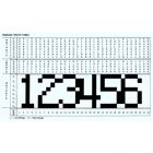
1965-4-----半导体只读存储器芯片的出现 半导体只读存储器(光盘)提供高密度和低成本的单位比特 作为在制造过程中被写入只读存储器的永久数据,使用光盘存储的信息,在整个系统的生命历程中,将保持不变,如微程序代码,查找表,字符代码等。集成电路光盘由放置在行和列组织的信号线之间的二极管阵列组建成。晶圆制造过程中的最后一步是把以实现客户的代码所需的具体二极管连接起来。作为一个最小的存储单元结构的二极管, ROM 器件提供毎比特最高的密度和最低成本的半导体存储器。 在 1965 年,西尔韦尼亚为霍尼韦尔生产了一个 256 位的双极 TTL 电光盘,它由工厂里熟练的技术人员在一段时间内编写的,该人员从事把物理划片的金属环连接到选定的二极管的工作。定制面罩编程设备的生产订单是令人满意的。在 1965 年总微电子还开发速度较慢,但 四倍 1024 位光碟使用 MOS 技术。在 20 世纪 70 年代初,仙童,英特尔,摩托罗拉, Signetics 公司和 TI 提供 1024 位 TTL 光盘,而 AMD 公司, AMI ,电子阵列,通用仪器,国家,罗克韦尔和其他一些公司提供 4096 位( 4K ) MOS 器件。 首次大批量应用的桌面计算器消费被来自美国和日本厂商的设备其采用亿万 16K 和更大的器件视频游戏墨盒所超越。任天堂的超级马里奥兄弟 NES 游戏单独的生产超过 4000 万单位。由于每个 ROM 有顺序的被供应,客户经常为较长的交货时间和供应商的供货不及时而感到沮丧,以用户可编程的光盘( PROM 的)的形式来缓解。 Credit: Fairchild Camera Instrument Corporation 256-bit ROM number generator programming table 256位ROM数发生器编程表 Courtesy of: Intel Corporation Intel 3301, 1024-bit Bipolar ROM 英特尔3301 , 1024位双极光盘 CHM Collection. Electronic image gift of William Blair Electronic Arrays 8316F 16K MOS ROM with package lid removed 电子阵列8316F 16K MOS去掉包盖的 ROM CHM Dan Rose Packaging Collection. Gift of SEMI Atari video game cartridge board with AMD 4K-bit MOS ROM circa 1982 雅达利游戏机墨盒板与AMD的4K位MOS ROM大约在1982年 译者:哈尔滨工业大学(威海)电子封装 090840211-杜伟 校对:哈尔滨工业大学(威海) 高阳 原文 http://www.computerhistory.org/semiconductor/timeline/1965-ROM.html 版权 copyright by www.nobeprize.org 英文原文 1965 - Semiconductor Read-Only-Memory Chips Appear Semiconductor read-only-memories (ROMs) offer high density and low cost per bit. As data is permanently written into a Read Only Memory during the manufacturing process, ROM storage is used for information that will remain unchanged throughout the life of a system, such as microprogram code, look-up tables, character generation, etc. Integrated circuit ROMs are built from arrays of diodes placed between signal wires organized in rows and columns. The last masking step of the wafer fabrication process makes connection to the specific diodes required to implement the customer's code. As a diode represents the smallest possible memory cell structure, ROM devices offer the highest density and lowest cost per bit form of semiconductor memory. In 1965 Sylvania produced a 256-bit bipolar TTL ROM for Honeywell that was programmed one bit at a time by a skilled technician at the factory who physically scratched metal link connections to selected diodes. Production orders were satisfied with custom-mask programmed devices. Also in 1965 General Microelectronics developed slower but four-times larger 1024-bit ROMs using MOS technology. By the early 1970s Fairchild, Intel, Motorola, Signetics, and TI offered 1024-bit TTL ROMs, while AMD, AMI, Electronic Arrays, General Instrument, National, Rockwell and others produced 4096-bit (4K) MOS devices. Desktop calculator consumption, the first high-volume application, was surpassed by video game cartridges that used hundreds of millions of 16K and larger devices from U. S. and Japanese vendors. Production of Nintendo’s first Super Mario Brothers NES game alone exceeded 40M units. As each ROM is manufactured to order, customers were often frustrated with long delivery times and vendors overwhelmed by production logistics. Relief came in the form of user-programmable ROMs (PROMs). ( 1971 Milestone )
 标签: 博物馆