一般高纯钛是指纯度在4 N 以上的钛 。作为钛系列产品中的一员,高纯钛以其优异的性能,主要应用于超大规模集成电路和真空设备的靶材中。在半导体领域中,高纯钛以钛硅化合物、氮化钛化合物、钨钛化合物等形式用于电极、扩散阻挡、配线等材料中,然而高纯钛中的杂质元素(例如:铁、镍、钠、钾等)超过一定含量会引起产品漏电流增大、性能下降等 。随着半导体电路集成度的不断提高,对高纯钛中所含杂质的含量要求越来越低。国外对有关高纯钛的研究较多 ,然而我国国内则相对很少。因而进行高纯钛方面的研究,具有非常重要的现实意义。 CVD 高纯钛就是以化学气相沉积的方法来制备高纯钛。利用卤素单质与粗钛在低温条件下经化合反应,生成气态卤化钛,通过传质过程,气态卤化钛扩散到沉积基体附近;在高温条件下,气态卤化钛在沉积基体表面分解为钛和卤素单质,钛在基体上结晶析出,最后得到钛晶体。晶体主要是由结晶作用形成。结晶是晶体在液体、气体等中从无到有(晶核形成)、由小变大(晶核长大) 的过程,结晶作用的方式主要有三类:(1气—固结晶(2)液—固结晶(3)固—固结晶。气—固结晶则是气态物直接转变为固态的晶体 。 本文依据经典的成核理论,对高纯钛的结晶成核过程进行热力学和动力学分析;根据所得到的热力学和动力学理论,对影响高纯钛结晶成核的主要因素进行分析;并讨论了影响钛沉积速率的原因。 4、结论 (1)对钛的结晶成核过程,进行热力学和动力学分析,得到钛结晶成核的热力学和动力学方程。从相应的数学方程分析可知,影响钛结晶成核的因素主要是沉积区温度和产物过饱和度。 (2)产物过饱和度和沉积区温度对成核自由能影响比较显著。随着产物过饱和度和沉积区温度增加,成核自由能减小,即越有利于结晶成核。 (3)钛的沉积速率随低价碘化物蒸汽压的升高而升高,因而蒸汽压是影响钛的提纯效果的重要因素, 实验过程中TiI2 的蒸气压应控制在60.8~101.3 Pa。 (4)分解区温度和卤化区温度对钛的沉积速率均有较大影响,其中在卤化区不只生成了卤化物,卤化区温度还同沉积区温度一起影响碘化物的转移速率,从而影响钛的沉积速率。 (5)反应过程中,高价卤化物的生成是消耗卤素、影响卤素使用效率的因素之一。高价卤化物的生成会影响低价碘化物的生成与转移,最终影响钛的沉积速率。 参考文献 石应江.高纯钛的生产与应用 . 上海金属(有色分册),1993,14(6):26- 33. 吴全兴. 高纯钛的制取 . 加工技术,1996(05):14- 16. 李哲,郭让民.高纯钛的制备及其发展方向 .钛业进展,1997(03). 【作者】 梁佰战; 李武斌; 曾英; 王舟; 【Author】 LIANG Bai-zhan,LI Wu-bin,ZENG Ying,WANG Zhou(College of Materials and Metallurgy,Guizhou University,Guiyang 550003,China) 【机构】 贵州大学材料与冶金学院; 【摘要】 采用化学气相沉积(CVD)法制备高纯钛。以经典的成核理论为依据,对钛在沉积基体上的成核过程进行热力学和动力学分析,计算出成核过程吉布斯自由能ΔGmax、成核速率v和临界晶核直径D0的数学方程;并且考察了影响钛沉积速率的因素,结果表明:卤化区的温度、分解区的温度、低价碘化物和高价碘化物的蒸汽压都对钛的沉积速率有一定的影响,其中两区的温度对钛的沉积速率影响较大。 【Abstract】 High-purity titanium was prepared via CVD(chemical vapor deposition) process.Based on the classical nucleation theory,the nucleation process of the titanium deposited on substrate was investigated thermodynamically and kinetically.Some relevant equations were thus derived,ie.,the Gibbs free energy(ΔGmax),nucleation rate(v) and critical crystal nucleus diameter(D0),and the influencing factors on the deposition rate of the titanium were discussed.The results showed that the halogenated area temperature,decomposed area temperature and the vapor pressures of low-valent iodide and high-valent iodide all have influence on the deposition rate of high-purity titanium,especially the temperature in halogenated and decomposited areas. 【关键词】 CVD; 高纯钛; 成核; 热力学; 动力学; 【Key words】 CVD; high-purity titanium; nucleation; thermodynamics; kinetics; 原文链接: CVD高纯钛成核热动力学及钛沉积速率分析 http://www.chvacuum.com/application/film/042378.html
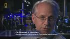
人工合成金刚石开启地球深部新视窗 (编译:周春银;原文作者: Tetsuo Irifune and Russell J. Hemley ;资料来源: EOS from AGU ) 【背景阅读】 2011 年 2 月我曾在博客中介绍日本科学家合成最硬人造金刚石的相关科普资料,见博文 《世界上最硬人造金刚石是如何炼成的》 。在该博文后,非常感谢有朋友(如“ anonymity ”)提到美国卡内基实验室 CVD 合成单晶金刚石的相关报道,不过限于本人知识水平有限,难于面面俱到作深入讨论。 关于金刚石的合成,国家地理曾经有一个 《 Super Diamonds 》 的纪录片,拍摄于 2009 年,如果大家感兴趣的话,可以去看一下,讲述了天然金刚石的来源、金刚石的高压合成和 CVD 合成法,以及金刚石的运用。我电脑里有一个 306 MB 的版本,还算比较清晰,不过中文字幕有好多错误和不当翻译。纪录片中有对美国卡内基实验室的 Hazen 、 Hemley (也是本文英文原作者)等顶尖级科学家以及著名的 Element Six 的采访和介绍,影片截图如下: 关于人工合成金刚石,最近又有一些新的进展,在正文开始之前,再稍微做一点介绍。博文 《世界上最硬人造金刚石是如何炼成的》 所提到的日本科学家高压合成的金刚石,研究人员正在努力使其“长大”和做一些开发工作(下面的正文中会提到一些)。首先,日本爱媛大学利用合成的超硬金刚石成功制作了直径 7.5mm 的金刚石真球体( http://www.ehime-u.ac.jp/research/news/detail.html?new_rec=8793 ),该金刚石真球体的制作,在某种程度上代表了日本科学家在该领域的研发实力,见下图。其次,爱媛大学和住友重工的成功合作,住友与 2012 年 2 月已经开始发售有关合成金刚石的工业制成品,如切削工具,见 http://www.sei.co.jp/news/press/12/prs006_s.html 。目前,进一步的研发还在继续进行中。 关于日本爱媛大学人工合成金刚石的研发工作,日本爱媛大学的 Tetsuo Irifune 教授曾经在 2011 年 12 月 7 日 AGU fall meeting 的“ 50 Years of High-Pressure Studies of the Earth ”分会场中(这一分会场为具有隆重的“ 毛河光 ”气氛,因为毛先生刚刚度过 70 岁生日并亲自到会场就坐听报告,会场上聚集了许多当今高压科学界和地学界的顶级科学家,包括毛先生女儿 Wendy Mao 在内的许多科学家高度赞扬了毛先生在高压科学研究中的卓越贡献,见 https://www.gl.ciw.edu/content/2011/12/9/ho-kwang-mao-honored-agu-fall-meeting-session ),专门介绍最新合成的金刚石 NPD 在未来的(尚处试验开发中)下一代高压装置中的运用研发情况( Title :“ Multiple Diamond Anvil (MDA) apparatus using nano-polycrystalline diamond ” ),大家可以登录 AGU 网站( http://sites.agu.org/fallmeeting/scientific-program/sessions-on-demand-7-december/ ) 或者 http://vimeo.com/33331037 观看(时间段: 47:54 至 59:59 )。 2012 年 2 月 14 日 AGU 的 EOS 刊发 Tetsuo Irifune 和 Russell J. Hemley 对人造金刚石的研发进展的最新文章(文章题目:“ Synthetic diamond opens windows into the deep Earth ”, EOS 链接: http://www.agu.org/pubs/eos/ ;其实在 T. Irifune 的 AGU 报告最后一张幻灯片中当时他本人已有提示这篇 EOS 文章即将和大家见面,见 59:30 处),或许大家可以从中得到一些启示,同时也是学习。我将该文章全文翻译,希望对大家有所益处。如果读者已经了解以上这些内容,将会十分有助于对本文内容和人工合成金刚石的理解认识。 以下为原文完整翻译,图文并茂: ------------------------------------------------------------------------------------------------------ 金刚石,由于其非凡的强度和透光性,在极端压力和温度条件下材料的实验研究中具有特别重大的作用。曾经,我们所使用的金刚石的质量和大小都受限于大自然。但是,研究人员现在已经可以在实验室中人工合成各种类型的金刚石了,它们更加坚韧而且体积比天然金刚石更大。 这些合成金刚石的性质特征使得科学家能够在从地表到地心范围压力 - 温度条件下研究物质材料。诚然,这些人工合成金刚石开启了地球深部的新视窗。 地球深部研究中的金刚石 绝大部分天然金刚石都是伴随着岩浆的喷发而被带到地表来的,这些岩浆来源于地下大约 150-200 公里深度(相当于 5-7 × 10 9 Pa 压力,或者海平面处压力的 5-7 万倍)。除了其非凡的强度和透光性之外,金刚石的化学稳定性使其成为将物质从地球内部带到地表的一个独特的载体( capsule )。通过对筛选出来的天然金刚石的包体的研究发现了很多高压矿物,说明这些物质来源于下地幔,即 660 公里以下深度 (图 1 ) 。因此,金刚石为下地幔和转换带的性质特征研究提供了非常重要的信息。 图 1. 地球内部切面指示金刚石(右上图)以及金刚石矿物包体(右下图;由 Ben Harte 和 Jeff Harris 提供)被发现的相对深度。大部分单晶金刚石来源于上地幔的上部(大约 150-200 公里深度)。而且,还有些天然金刚石含有矿物包体,如 majorite 石榴子石,铁方镁石,硅酸镁和硅酸钙,所有这些矿物被认为形成于地幔转换带( 410-660 km 深度之间)和下地幔深部。另外,气相化学沉积法( CVD )金刚石和纳米聚晶金刚石( NPD )压砧新技术使得科学家可以对下地幔最深部( D” 层)和地核物质开展研究,目前还缺乏如此深度的来自天然金刚石的样品。 从另一方面来说金刚石也为地球深部开启了一个重要的窗口:金刚石是高压仪器中的一种重要砧头( anvil )材料——像金刚石类似的坚硬物质,在将样品压缩到与行星深部相应条件的过程中非常重要。金刚石压砧( diamond anvil cells, DACs ),将两颗单晶金刚石作为对顶砧头,能够产生超过 364 × 10 9 Pa 压力(相当于地心处的压力)。由于金刚石具有很高的透光性,样品在高压条件下的性质可以通过这个窗口而被我们观测到。在过去的三十多年里 DAC 的前沿研究,包括在地球核幔边界区压力和温度条件下发现的后钙钛矿相(地幔主要成分铁镁硅酸盐的一种高压形式) ,为深部地幔和地核组成物质的晶体结构、熔融作用、元素分异以及其他性质特征提供了重要的信息。 首个在实验室中成功合成的金刚石报道于 20 世纪 50 年代中期(如 Bundy et al.,1955 ),随后即投入到为工业运用服务的商业生产中。近年来,利用不同的技术,两种新的金刚石材料分别在美国华盛顿卡内基研究所地球物理实验室和日本松山市爱媛大学的地球动力学研究中心( Geodynamics Research Center )被合成出来。前一种是在高生长速率和低压条件下生成的大颗粒单晶金刚石。后一种,称为纳米聚晶金刚石( Nanopolycrystalline Diamond , NPD ),由超细的纯金刚石颗粒烧结而成,更加坚韧而且通常比天然金刚石更硬。 化学气相沉积法的单晶金刚石合成 天然金刚石可以是单晶或者聚晶,高级别的单晶是光学透明的,可以用作宝石,而聚晶则更加趋向于暗色,或者由于许多包体以及颗粒边界处杂质的存在而呈半透明。尽管两种金刚石都具有极好的硬度,而单晶金刚石比大部分聚晶金刚石具有更高的强度,但是它们也可能沿某些晶面而开裂。聚晶金刚石因为微细晶粒间具有很强的粒间结合力而通常韧性更高。这些特征使得其在工业运用中非常实用,如作切削工具。 利用化学气相沉积法( chemical vapor deposition , CVD )合成聚晶金刚石报道于 20 世纪 60 年代。但是结果仍不确定而且生长速率非常低(大约每小时 1mm )。另外,还只能做成非常薄的膜,而它们往往强度很弱且不均匀。 传统的单晶金刚石的合成是利用特定的催化剂和溶剂在接近于石墨 - 金刚石相边界的压力和温度条件下(大约 5-6 × 10 9 Pa , 1500 K )进行的。利用专门的、精细控制的大压机,高质量的单晶金刚石也有被合成出来。纯的无色的单晶金刚石有被合成出来;这些单晶金刚石的某些特定晶面据报道具有很高的硬度,但是体积大小仍受限于几个毫米 。由于生长速率非常缓慢,以及用来合成金刚石的高压设备对样品体积的限制,要合成较大的单晶金刚石非常困难。利用微波等离子 CVD (大气压之下)单晶金刚石的生长技术于二十世纪 90 年代后期在卡内基地球物理实验室被开发出来。而且,生长速率甚至高达每小时 150 mm ,这一速率比聚晶 CVD 方法高两个数量级 。从此以后,体积更大、质量更好的单晶金刚石通过不断优化生长和合成后期处理,如高温高压退火处理,而被合成出来 (图 2 ) 。 直径达 2.5 厘米的单晶金刚石( 10 克拉)现在已经在卡内基地球物理实验室被成功合成出来。最纯的 CVD 金刚石的紫外线 - 可见光吸收谱特征与高纯天然金刚石晶体是一样的 。它具有和纯的无缺陷的金刚石相似的硬度。更加重要的是,通过控制生长和退火工艺可以合成具有高韧性的金刚石 。因此,相对于传统单晶金刚石而言, CVD 单晶金刚石可以说是一种功能更为强大有用的材料。 图 2. 两种新型金刚石的合成和运用。(顺时针从左上角)在美国华盛顿卡内基研究所地球物理实验室用 CVD 技术合成的大颗粒单晶金刚石样品(直径超过 1 厘米,或 2.4 克拉)( Y. Meng 提供)。透过 CVD 反应器窗口对 900 C 和低于一个大气压条件下正在生长的金刚石晶体所拍摄的照片;金刚石为大约 8mm 的晶片( K. Hemawan 提供)。图示金刚石压砧装置的压砧构架,其中样品由两个对顶放置的单晶金刚石压缩,利用新型 CVD 金刚石材料可以产生更高的压力和温度( J. Shu 提供)。利用脉冲激光将纳米聚晶金刚石( NPD )圆柱切割成立方体,目前这些金刚石立方体正在被测试用作下一代多面砧装置的压砧材料。日本爱媛大学地球动力学研究中心安装的新 6000 吨多面砧装置,目前正用于 NPD 材料的合成研究。直径和长度均达 1 厘米的 NPD ( 14.5 克拉)圆柱样品。 纳米聚晶金刚石 NPD 聚晶金刚石在自然界中有被发现,但是通常结构不强而且不透明。一般而言在高压条件下烧结材料可以增强其特征性质。但是长期以来,在高压条件下合成纯的烧结的聚晶金刚石仍然是一大挑战,因为金刚石粉末的烧结极其困难。因此,只有那些含有诸如钴粘结剂的聚晶金刚石在高压下被合成出来并用于工业和科学用途。 爱媛大学地球动力学研究中心利用大体积压机开发出了新的方法 。在这种方法中,石墨在大约 15 × 10 9 Pa 和超过 2600 K 的条件下(比传统高压方法高很多)直接转变成为金刚石,形成纳米聚晶金刚石( NPD )。通过运用如此高的压力和温度条件(远远高于石墨 - 金刚石平衡边界),迅速生成大量纳米级的金刚石颗粒,可以在几分钟内合成一个烧结极好的 NPD (图 2 ) 。 现已研究发现, NPD 具有和大部分单晶金刚石相似的甚至更高的硬度,同时也具有很高的弹性刚性和相对较低的热导性。对于砧头非常重要的是, NPD 具有非常高的破裂韧性。 NPD 对可见光和红外光也具有高穿透性,除了大约 700 纳米以下的短波,因此显示为暗黄色的颜色。直径和长度均达 1 厘米( 14.5 克拉)的无裂隙 NPD 已在多面砧装置中被合成出来。 新金刚石的运用 除了广泛的工业用途,如用作切削加工,这两种新金刚石——单晶 CVD 和 NPD ,在高压地球科学中也具有广泛的运用。 单晶 CVD 金刚石已经在如压缩气体等材料的 DAC 实验中来提高其最高稳定压力 - 温度条件。例如关于氢在与类木行星深部相同条件下的研究,那里的压力可能高达几百个 GPa 。 另一项重要的用途则是在 DAC 中运用比传统金刚石体积更大的 CVD 压砧。尽管已有的激光加热 DAC 技术可以产生深部地幔和地核中的压力 - 温度条件,但是实验永远都是充满挑战。在高压下 DAC 样品非常薄,这使得材料的激光加热变得困难,因为金刚石的高热导会导致热量流失。通过使用体积更大、强度更高的材料做垫圈材料来产生更大的样品体积,这些问题可以尽量减小。样品的物性测量,如声速、电导和热导,在较大的 DAC 装置中会更加容易和精确。于是,这些装置将成为非常强大的工具来研究深达地球内核压力 - 温度条件下物质的相变、元素分异、熔融作用和物理性质。 开发的新 CVD 金刚石材料使得科学家创造出下一代的高压设备,包括设计用来提高各种功能的压砧。除增大样品体积之外,较大的单晶金刚石可以用于 X 光和中子散射测量——这两种技术均需要较大的样品 。另外,引入传感器和电路可以制作非常精细的用于电和热传输测量的压砧 。这些技术可以非常方便地运用于解决深部地球物理、地球化学和地球动力学等主要问题的实验中。这些材料的进一步开发有望形成新的地球和行星科学以外的基于金刚石的高科技,如开发电子传感器、激光和基于金刚石的计算机 。 NPD 已经成功运用于新的 DAC ,并产生了高达大约 250 GPa 和 5000 K 的压力温度调教 。在大约 150 GPa 的中等压力实验中, NPD 压砧,尤其是那些具有相对较大的底面、样品被包裹压缩起来的压砧,研究表明可以经受住与具有相同底面大小的单晶金刚石压砧两倍的压力 。研究还显示,在高温高压条件下, NPD 要比单晶金刚石的塑性变形小得多 。而且,当来自压砧的单晶衍射需要屏蔽时,如在某些 X 光吸收研究中 , NPD 相对于单晶金刚石更具优越性。 NPD 在 6-8 型多面砧装置运用中或许具有更加重要的作用,在一个大体积单轴压机装置里 8 个二级立方压砧被置于统一运作的 6 个一级压砧中。含有一些金属粘结剂的烧结聚晶金刚石现在已经被运用于这种压机的二级压砧,但是能产生的最大压力仍低于 100 GPa 。因为 NPD 的硬度是这些烧结金刚石集合体的大约两倍,那么当被用作二级压砧时,期待能更高的压力,至少 150 GPa ,而不需要牺牲多面砧装置的一些优点,如在相对较大的样品中具有均匀的压力和温度分布。因此,精确的高压矿物物理研究,例如准确确定地幔底部(大约 136 GPa 和 3000 K )附近铁 / 镁硅酸盐相的钙钛矿和后钙钛矿之间的相边界以及相应的密度密度或弹性特征的变化,可以用来和 DAC 测量结果对比。 新型材料 新型金刚石技术在地球科学研究中潜力的开发才刚刚开始,但是非常具有前景的单晶 CVD 金刚石和 NPD 压砧在各种高压设备中的运用已经展开。目前的努力探索在于合成体积更大、质量更高的金刚石。这些由地球物理学家而发明的新型材料,为探索行星内深部区域开启了新的窗口并具有更高的精度、分辨率和灵敏度,而且还将运用于地球科学以外的科学研究。 参考文献 Bundy, F. P., H. T. Hall, H. M. Strong, and R. H. Wentorf Jr. (1955), Man-made diamonds, Nature, 176, 51 – 55. Harte, B., and J. W. Harris (1994), Lower mantle mineral associations preserved in diamonds, Mineral Mag., 58A, 384 – 385. Irifune, T., A. Kurio, S. Sakamoto, T. Inoue, and H. Sumiya (2003), Ultrahard polycrystalline diamond from graphite, Nature, 421, 599 – 600. Kunimoto, T., T. Irifune, and H. Sumiya (2008), Pressure generation in a 6-8-2 type multi-anvil system: A performance test for third-stage anvils with various diamonds, High Pressure Res., 28, 237 – 244. Liang, Q., C. S. Yan, Y. Meng, L. Lai, S. Krasnicki, H. K. Mao, and R. J. Hemley (2009), Recent advances in high-growth rate single-crystal CVD diamond, Diamond Related Mater., 18, 698 – 703. Matsumoto, K., H. Maruyama, N. Ishimatsu, N. Kawamura, M. Mizumaki, T. Irifune, and H. Sumiya (2011), Noncollinear spin structure in Fe-Ne invar alloy probed by magnetic EXAFS at high pressure, J. Phys. Soc. Jpn., 80 (2), 023709-1 – 023709-4, doi:10.1143/ JPSJ.80.023709. Meng, Y. F., C. S. Yan, S. Krasnicki, Q. Liang, J. Lai, H. Shu, T. Yu, A. S. Steele, H. K. Mao, and R. J. Hemley (2012), High optical quality multicarat single crystal diamond produced by chemical vapor deposition, Phys. Status Solidi A, 209 (1), 101 – 104. Murakami, M., K. Hirose, K. Kawamura, N. Sata, and Y. Ohishi (2004), Post-perovskite phase transition in MgSiO3, Science, 304, 442 – 445. Nakamoto, Y., M. Sakata, H. Sumiya, K. Shimizu, and T. Irifune (2011), High-pressure generation using nano-polycrystalline diamond as anvil materials, Rev. Sci. Instrum., 82, 066104. Ohfuji, H., T. Okada, T. Yagi, H. Sumiya, and T. Irifune (2010), Laser heating in nano-polycrystalline diamond to laser-heated diamond anvil cell experiments, High Pressure Res., 30, 142 – 150. Samudrala, G., W. Qiu, S. A. Catledge, J. G. Harrison, Y. K. Vohra, and S. T. Weir (2008), Growth chemistry for the fabrication of designer diamonds for high pressure research, High Pressure Res., 28, 1 – 8. Sumiya, H., N. Toda, and S. Satoh (2002), Growth rate of high-quality large diamond crystals, J. Cryst. Growth, 237-239, 1281 – 1285. Walter, M. J., S. C. Kohn, D. Araujo, G. P. Bulanova, C. B. Smith, E. Gaillou, J. Wang, A. Steele, and S. B. Shirey (2011), Deep mantle cycling of oceanic crust: Evidence from diamonds and their mineral inclusions, Science, 334, 54 – 57. Wang, S., et al. (2012), Single-crystal CVD diamonds as small-angle X-ray scattering windows for high pressure research, J. Appl. Crystallogr. , in press. Yan, C. S., Y. K. Vohra, H. K. Mao, and R. J. Hemley (2002), Very high growth rate chemical vapor deposition of single-crystal diamond, Proc. Natl. Acad. Sci. U. S. A., 99, 12,523 – 12,525. Zha, C. S., S. Krasnicki, Y.-F. Meng, C.-S. Yan, J. Lai, Q. Liang, H.-K. Mao, and R. J. Hemley (2009), Composite chemical vapor deposition diamond anvils for high-pressure/high-temperature experiments, High Pressure Res., 29, 317 – 324. ---------------------------------------------------------------------------------- 后注: 1. 在本文翻译中,我将 diamond 翻译成“金刚石”,而不是“钻石”,我认为“钻石”一词或许更多地运用于宝石领域,而本文则主要是材料学和高压地球科学,因此取“金刚石”的翻译;例如, diamond anvil cell 一般被翻译为金刚石压砧 / 腔。 2. nanopolycrystalline diamond 一词,我既有听到“纳米多晶金刚石”的翻译也有听到“纳米聚晶金刚石”的翻译方式,哪位朋友或者老师如果知道有比较专业通用的翻译,请留言告诉一下,谢谢。
有兴趣的可以看看下面我的博客文章: 1) http://www.sciencenet.cn/blog/user_content.aspx?id=402561 ( 关 于(微波法)CVD金刚石膜产业化的看法 ) 2) http://www.sciencenet.cn/blog/user_content.aspx?id=231983 ( 金刚石薄膜的性质、制备及应用 ) 3) http://www.sciencenet.cn/blog/user_content.aspx?id=232233 ( 微波等离子体化学气相沉积—— 一种制备金刚石膜的理想方法 ) We’re starting to lay down thick layers of diamond in CVD machines, hinting towards a future of bulk diamond machinery. Diamond is an ideal construction material — it’s immensely strong, light, made out of the widely available element carbon, nearly complete thermal conductivity, and has among the highest melting and boiling points of all materials. By introducing trace impurities, you can make a diamond practically any color you want. Imagine a jet, with hundreds of thousands of moving parts made of fine-tuned diamond machinery. Such a craft would be more powerful than today’s best fighter planes in the way an F-22 is better than the Red Baron’s Fokker Dr.I. 这里有我上传的美国一家公司生产CVD钻石的视频介绍: 看看老外关于CVD制备钻石的视频 http://bbs.sciencenet.cn/forum.php?mod=viewthreadtid=201614extra=page%3D1 CVD金刚石膜的制备方法主要有四种:热丝法,微波法,直流电弧法和燃烧火焰法,其中微波法是高端金刚石膜应用的最理想方法。下面主要就微波法制备的产品及品质,应用进行分析,大部分数据都是从网络上来的,呵呵! 微波法优于等离子体靠电磁波激发,避免的电极的污染,因此可以制备高纯度的金刚石膜。 上图就是微波法同质外延金刚石(单晶钻石)的情形 图片中的是生长用的“种子”,一种特别加工的金刚石仔晶。经过CVD过程,可以将大自然几百万年过程生成的金刚石,压缩到很短的时间,就能在实验室里面生长出钻石级的金刚石,而且完美无缺,比最好的天然金刚石还要好。下图就是生长前后的照片。 该技术的关键是:可以在很短的时间内作出完美无缺的大颗粒钻石级别的金刚石;更重要的是该技术能批量生产;这完全不同于高温高压法的一次就只能生产一颗,而且由于含有金属催化剂,一般作出来的都是黄色的“黄钻”。 这些是CVD法制备的钻石级金刚石,颜色的选择性出现是在生长国产中人为掺入了一些着色物质。其制备成本都是差不多的。 下图是高温高压法(HTHP)制备金刚石的现场照片: 下面是用HTHP方法制备出来的钻石照片: CVD技术,可以在制备金刚石膜的同时加入一些“染色剂”,可以认为的制备出不同颜色的金刚石。 下面就是引用元素六公司的产品( http://193.120.252.126/cvd/page.jsp?pageid=298 ): 1) Optical Grade CVD (OP) (光学级金刚石膜) Optical grade polycrystalline CVD diamond. Broad transparency, high thermal conductivity, durable and wear resistant. Suitable for use in IR and high power laser optics. (价格单位是:英镑) Thermal Management Grade CVD (金刚石膜散热片) Thermal management grade polycrystalline CVD diamond with a thermal conductivity 1000 Wm-1K-1. Mechanical Grade CVD (PC) (机械级CVD金刚石膜) PC Grade CVD is used extensively for precision cutting tools and scalpels. Electrochemistry Grade CVD (PE) (导电金刚石膜) Electrically conductive polycrystalline CVD suitable for use in electrochemistry applications. This material can also be cut by EDM. Single Crystal Diamond Plate (单晶金刚石膜) 其他的就不黏贴了,反正CVD金刚石膜可以通过微波法做得非常的好。至于市场,大家可以积极参与,共同开发。 下面是一些CVD产品,网上图片,仅供参考: The ability to process large size transparent windoews in diamond with consistant quaility is key to its application in advanced optics Diamond is the only material that offers a wide far-infrared (8-14 um) range transmission combined with high strength and excellent resistance to thermal shock, scratching and erosion The use of CVD diamond optics in high power laser applications overcomes the common problem of thermal distortion of the beam by the window material. The broad-band optical transparency , high thermal conductivity and hardness make diamond an ideal choice for highly demanding window applications such as high-power IR laser windows, high-power microwave windows and durable windows for aggressive environments. Its optical transparency covers the whole spectral range from the UV to the far infrared. Specifications for standard diamond windows Diamond windows can be manufactured to the following standard specifications. 下面图片出自: http://www.diamond-materials.com/prod_overview_en.htm ,具体详情可以自己去看看。市场前景很大,只要能做得出来。他们都是用微波法生产的。 千万不要用老思维方式看如何工业化生产CVD金刚石膜,这些高科技东西第一要求的是质量,而不是数量,质量达到要求了,可以从某种程度上讲不用说价格,一定有人买的。一句话:不怕你卖不出去,就怕你做不出来! 如果需要CVD金刚石膜设备,可以与我联系,可以根据要求进行配置,从而满足不同的科研,教学的要求。 热丝CVD或者各种功率大小的微波CVD均可以与我联系!喜欢CVD金刚石膜的朋友,可以看我博客中的其他文章。 ----------------------------------------------------------------------------- 欢迎看看我的其他的博客内容: 金刚石薄膜的性质、制备及应用 http://bbs.sciencenet.cn/home.php?mod=spaceuid=257140do=blogid=231983 微波等离子体化学气相沉积 —— 一种制备金刚石膜的理想方法 http://bbs.sciencenet.cn/home.php?mod=spaceuid=257140do=blogid=232233 微波 CVD 金刚石膜产品及应用分析 http://bbs.sciencenet.cn/home.php?mod=spaceuid=257140do=blogid=402659 关于(微波法) CVD 金刚石膜产业化的看法 http://bbs.sciencenet.cn/home.php?mod=spaceuid=257140do=blogid=402561 Carnegie-Made Diamonds on Exhibit(CVD 金刚石产品展示) http://bbs.sciencenet.cn/home.php?mod=spaceuid=257140do=blogid=386101 国外先进的微波等离子体 CVD 制备金刚石膜设备介绍 (Diamond) http://bbs.sciencenet.cn/home.php?mod=spaceuid=257140do=blogid=384330 微波等离子体 CVD 制备金刚石膜 http://bbs.sciencenet.cn/home.php?mod=spaceuid=257140do=blogid=384313 Synthetic Diamonds http://bbs.sciencenet.cn/home.php?mod=spaceuid=257140do=blogid=351296 微波等离子体同质外延修复金刚石的研究 http://bbs.sciencenet.cn/home.php?mod=spaceuid=257140do=blogid=232229 微波 CVD 金刚石薄膜用作 LED 散热片的制备 http://bbs.sciencenet.cn/home.php?mod=spaceuid=257140do=blogid=232213 提高金刚石薄膜与硬质合金基底之间附着力工艺的研究进展 http://bbs.sciencenet.cn/home.php?mod=spaceuid=257140do=blogid=231988 国外微波法制备金刚石膜设备介绍( microwave plasma CVD diamond system introduction) http://bbs.sciencenet.cn/home.php?mod=spaceuid=257140do=blogview=mefrom=spacepage=2 等离子体技术 —— 一种处理废弃物的理想方法 http://bbs.sciencenet.cn/home.php?mod=spaceuid=257140do=blogid=259594
本文最后有关于微波设备的联系方式,关于微波CVD金刚石膜产业化的问题,可以看我的博客文章: http://www.sciencenet.cn/blog/user_content.aspx?id=402561 ( 关于(微波法)CVD金刚石膜产业化的看法 ) 看看老外用微波设备作材料研究的视频: http://bbs.sciencenet.cn/forum.php?mod=viewthreadtid=201615extra = AX5010 Microwave Plasma CVD Reactor (1.5 kW) The AX5010 Microwave Plasma CVD Reactor is used for growth of high quality diamond films. Intended as a low cost system for basic film research in RD laboratories. It produces a wide range polycrystalline and single crystal diamond films on a variety of substrates with properties equal to or better than those made by any other method. The AX5010 is easy to use, small in size, and gives reproducible results. Model AX5010 AX5200 1.5kW Microwave Plasma CVD Integrated System he model AX5200 Microwave Plasma CVD system incorporates a 1.5kW at 2.45GHz microwave generator for high power and high temperature plasma deposition. System can also be equipped with optional electromagnets to become an Electron Cyclotron Resonance (ECR) system for operations at low pressure and low temperature. Both systems are: Capable of depositing high quality CVD diamond films for a wide variety of applications Flexible reactor design supports high pressure microwave and magnetized microwave CVD Development time minimized with supplied CVD diamond process recipes Reliable, stable, reproducible, versatile operation Modular approach to suit a wide range of budgets Manual operations or Computer controlled GUI for ease of operation Up to 6 different gas inlets Pressures from 10 to 150 Torr (1 to 150 Torr optional) Substrate Stage Temperature control – heated stage Extensive after-sales support AX5200 1.5kw Integrated Systems AX5250 5kW Microwave Plasma CVD System The AX5250 microwave plasma reactor incorporates a 5kW at 2.45GHz microwave generator to produce plasma at high power densities. Such operation allows a new regime of plasma chemistries. In this microwave cavity configuration, liner growth rates on axis up to 15 micro meter an hour for diamond have been demonstrated. Total mass deposition rates of 60mg/hour have been achieved. The process recipe for thick, high growth films is included with the system. Features: Film or thick CVD diamond at deposition rates up to 15 micro meter per hour White transparent diamond at growth rates up to 2 to 5 micro meter per hour. Accommodates substrates up to 4 inch diameter Produce CVD diamond with high thermal conductivity - 10 to 20 W/cm-K Operation at 10 to 100 Torr (1 to 100 Torr optional) Fully automated for CVD diamond growth for multi-recipe, multi-day operation AX5250 5kW Integrated Systems Comparison between 1.5kW and 5kW Microwave Diamond CVD Microwave Power 1.5kW 5kW Appropriate applications Semiconductor device (doping), Homo Hetero epitaxial films, FED* Thermal management (Heat Sink), Optical, Tools coating, FED*, SAW filters** Typical Growth rate 0.1 - 0.5 or 1 micron/hr 2 - 5 or 6 micron/hr Substrate Stage Heated Stage Water Cooled Stage Substrate Temp. Control Digital Setting Need shim replacement BEN*** OK OK Grain Size Small Small - large Sample size 50mm (2 inch)±15% uniformity (Guaranteed) 50mm (2 inch) ±15% uniformity (Guaranteed) Accommodating substrate 90mm (4 inch) 100mm (4 inch) Stage Option: No Yes (changeable to heating stage) Field Emission Display*, Surface Acoustic Wave**, Biased Enhanced Nucleation*** AX6500 8kW Microwave Plasma CVD System The AX6500 produces CVD diamond substrates suitable for most heat-spreading applications. Thick CVD diamond films, to over 3.5 inches in area, enable and expand applications such as laser diode mounts, multi-chip modules, surface acoustic wave devices, and high-power GaAs-based circuits. The AX6500 is designed for a production environment, with features including: easy loading, push-button operation, low maintenance and high uptime. The AX6500 high deposition rates allow relatively short deposition runs which increases manufacturing flexibility and response time. The AX6500 combines the most advanced microwave reactor design and high growth rate diamond deposition process into a turnkey system for pilot production of CVD diamond-coated tool inserts. In addition, the AX6500 is ideally suited for robotic tool handling in a production environment. Features: Deposits CVD diamond films at growth rates and uniformity necessary for practical, cost effective tooling applications Enables pilot production of CVD diamond-coated tools Provides a path to full-scale production Includes proprietary process knowledge which significantly shorten the user's learning curve. Easy to use Available with extensive after-sales service and support for high reliability and uptime AX6500 8kw Semi-Production Model AX6600 Microwave Plasma CVD System The AX6600 microwave plasma system is designed to operate with plasma at high power densities for large area, high deposition rate processes to meet the scale-up needs for diamond coated tool insert manufacturers. This complete turnkey system incorporates the latest microwave technology with computer control for ease of use. A large batch size, covering an area of 8 inches in diameter, can be processed all at once. It is a highly flexible design which can be operated in a wide range of power from 15kW to 100kW. Features: Large throughput Easy to use Production capability Computer-controlled, turnkey operation Reliable, stable reproducible,versatile operation Extensive after-sales process support and training Specifications of different models System Model AX5200 AX5250 AX6500 AX6600 Reactor Type Plasma Immersion Plasma Immersion Plasma Immersion Plasma Immersion Usage RD RD Production Production Stage Heated or Cooled Heated Cooled Cooled Cooled RF Power 1.5kW 5kW 8kW 60 - 100kW RF Frequency 2.45GHz 2.45GHz 2.45GHz 915MHz Typical Diameter 50mm 50mm 64mm dia. Thermal 100mm dia. Tools 200mm Max Diameter 100mm 100mm 125mm 300mm Typical Growth Rate 0.1-0.5μm/hr Up to 7μm/hr Up to 7μm/hr Up to 15μm/hr Typical Mass Rate 1-4mg/hr 60mg/hr 90mg/hr 1g/hr MPCVD FOR DIAMONDS PECVD system with reliable and versatile base and many options will solve almost any your RD problem. DIFS-ST10 system for MPCVD diamond film growth. Applications: tool coatings IR optical components heat spreaders for electronic devices surface acoustic waves devices biosensors, biocompatible coatings conductive diamond electrodes for electrochemistry ionizing radiation detectors (UV, X-ray, particles) MEMS The DIFS-ST10 microwave plasma CVD reactor is designed for polycrystalline diamond film and wafers deposition on large area substrates of various materials. Smooth nanocrystalline diamond films can be deposited as well. B asic parameters of the CVD system: Microwave power source: 5kW at 2.45 GHz. Number of feed gas channels: 4. Reaction gases: CH4, H2 (main); O2, Ar, N2, CO2 optional. Gas process pressure: 20-150 Torr. Gas consumption: 1000 sccm (typical). Substrate diameter: 3 inches. Substrate temperature: 700 – 1000°С (control with a pyrometer). Growth rate: 1-7 microns/hour. Diagnostic ports: 5 quartz windows. Vacuum chamber: stainless steel, water cooled. Full computer control. 5KW microwave plasma CVD system Reactor Parameters MW Power - 30 kW MW Frequency - 915 MHz Bell Jar Diameter – 10” (25 cm) Sample Holder Diameter – 6” (15 cm) Water Cooled Stage Optional Bias Voltage Temperature Control by IR-Pyrometer Optical Emission Spectroscopy Control Capable for long deposition hours Microwave plasma chemical vapor deposition chamber shown in action growing ultrananocrystalline diamond films at Argonne's Center for Nanoscale Materials. AsTex MWCVD MicroWave Plasma Chemical Vapour Deposition - Process gases: methane(CH4), hydrogen(H2), nitrogen(N2), argon(Ar), oxygen(O2) - Materials: Poly- and nanocrystalline diamond films (PCD and NCD) A Lamda Technologies microwave plasma-enhanced chemical vapor deposition (PECVD) instrument for the growth of nanocrystalline diamond is available in the cleanroom facility This system is an Electron-Cyclotron Resonance Plasma Enhanced Chemical Vapor Deposition (ECR-PECVD) chamber which we have used in research related to diamond and other carbon-based thin films, low-K dielectrics, and other thin films. This system uses a 2.45 GHz microwave source and a ring of rare earth magnets to create a plasma which is used to break down gaseous precursors and deposit films onto a variety of substrates. A 2.45 GHz, 1.5 kW, Microwave Electron Cyclotron Resonance (ECR) plasma processing facility has been set up to give a uniform deposition on a substrate area of around 100 mm, with features like substrate rotation, substrate heating, deposition under RF bias / pulse bias condition etc. The photo on the left shows the system undergoing tests. Diamond is grown from a plasma generated by a gaseous absorption of high power microwave energy Plasma Quest ECR Etch Tool 如果需要CVD金刚石膜设备,可以与我联系,可以根据要求进行配置,从而满足不同的科研,教学的要求。 热丝CVD或者各种功率大小的微波CVD均可以与我联系!喜欢CVD金刚石膜的朋友,可以看我博客中的其他文章。 --Options-- * Optical Emission Spectrometer * Remote Raman Spectrometer * Additional Gas Channels * Biasing capabilities * Temperature Measurement System (In-situ nucleation monitoring) * Turbo Pump ------------------------------------------------------------- 欢迎看看我的其他的博客内容: 金刚石薄膜的性质、制备及应用 http://bbs.sciencenet.cn/home.php?mod=spaceuid=257140do=blogid=231983 微波等离子体化学气相沉积 —— 一种制备金刚石膜的理想方法 http://bbs.sciencenet.cn/home.php?mod=spaceuid=257140do=blogid=232233 微波 CVD 金刚石膜产品及应用分析 http://bbs.sciencenet.cn/home.php?mod=spaceuid=257140do=blogid=402659 关于(微波法) CVD 金刚石膜产业化的看法 http://bbs.sciencenet.cn/home.php?mod=spaceuid=257140do=blogid=402561 Carnegie-Made Diamonds on Exhibit(CVD 金刚石产品展示) http://bbs.sciencenet.cn/home.php?mod=spaceuid=257140do=blogid=386101 国外先进的微波等离子体 CVD 制备金刚石膜设备介绍 (Diamond) http://bbs.sciencenet.cn/home.php?mod=spaceuid=257140do=blogid=384330 微波等离子体 CVD 制备金刚石膜 http://bbs.sciencenet.cn/home.php?mod=spaceuid=257140do=blogid=384313 Synthetic Diamonds http://bbs.sciencenet.cn/home.php?mod=spaceuid=257140do=blogid=351296 微波等离子体同质外延修复金刚石的研究 http://bbs.sciencenet.cn/home.php?mod=spaceuid=257140do=blogid=232229 微波 CVD 金刚石薄膜用作 LED 散热片的制备 http://bbs.sciencenet.cn/home.php?mod=spaceuid=257140do=blogid=232213 提高金刚石薄膜与硬质合金基底之间附着力工艺的研究进展 http://bbs.sciencenet.cn/home.php?mod=spaceuid=257140do=blogid=231988 国外微波法制备金刚石膜设备介绍( microwave plasma CVD diamond system introduction) http://bbs.sciencenet.cn/home.php?mod=spaceuid=257140do=blogview=mefrom=spacepage=2 等离子体技术 —— 一种处理废弃物的理想方法 http://bbs.sciencenet.cn/home.php?mod=spaceuid=257140do=blogid=259594
 标签: CVD