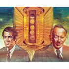
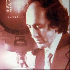
有关 Mervin Joe Kelly 先生的网页 Kelly, Mervin J. : Photographic Archive - University of Chicago http://photoarchive.lib.uchicago.edu/db.xqy?one=apf1-03156.xml (1)童诗白,2001-05,世纪回眸:纪念晶体管的发明和由此引出的启发 《电气电子教学学报》,2001年6月,第23卷第3期:3-6,20 http://www.cnki.com.cn/Article/CJFDTotal-HHGY2001S1000.htm 有鉴于此,当时贝尔的实验室主任 Kelly 根据19世纪以来关于半导体在光照下能产生电流以及它和金属接触能起到整流和检波作用的现象, 认为半导体有希望能取代电子管。 为此,要加强对固体物理基础理论的研究。从1936年起开始招聘有关的尖端人才,组成研究小组。 (2)搜狐,2019-01-28,你也许没想到,现代科技的半壁江山都由这个实验室打造 http://www.sohu.com/a/292034869_465246 他的基本信条是:一个“创新科技研究所”——正如他拥有的贝尔实验室那样,需要足够多的天赋异禀的人不断地交换思想。但是真正要创新,这些还不够。Kelly 先生坚信面对面交流的重要性。通过电话交换思想?不行!他故意把贝尔实验室的思想者和实践者集中在同一屋檐下。在晶体管开发项目中,有目的地将物理学家,冶金学家,电器工程师混合在一个项目组里,项目组中的每个人都各自是理论、实验或者制造领域的专家。像一个老练的交响乐指挥一样,Kelly 先生在科学定律之间,研究院和开发者之间,个人和团队之间游刃有余,时而寻找和谐,时而要求张力。 Kelly 先生相信自由的重要性,尤其是在科研方面。他手下的许多研究人员拥有如此之高的自主权,以至于项目进度拖后了长达数年,Kelly 都没有意识到。举个例子, 最早是他挑选了一队研究员成立了半导体项目组。当最后半导体被发明出来的时候,其实项目已经延期两年了。 随后,他设立了另一个研究小组,主要负责半导体的批量生产。他把这个任务委托给了其中的一个工程师,指示他做出计划,随后他就告诉这个工程师,自己即将去欧洲出差了,项目由这个工程师全权负责。 (3)Mervin Joe Kelly - National Academy of Sciences http://www.nasonline.org/member-directory/deceased-members/20000623.html Mervin J. Kelly, February 14, 1894 - March 18, 1971 Election Year: 1945, Membership Type: Member http://www.nasonline.org/member-directory/deceased-members/20000623.html He wanted, found, appreciated, and encouraged the sort of men who invented the transistor. William Shockley has said, Kelly's stimulus to look for new devices useful in the telephone business, plus exposure to new theories about rectification mechanisms in copper oxide, led me to invent a structure that would have worked as a transistor. (4)Mervin Joe Kelly - American Institute of Physics https://history.aip.org/phn/11602035.html (5)Presidents of Bell Labs https://www.bell-labs.com/about/history-bell-labs/presidents/ Mervin Kelly, President 1951–1959 He pioneered the methods of industrial research, of “inventing ways to invent things.” His tool kit included cross-disciplinary teams of experts, close proximity between researchers and developers and even ways to design buildings to encourage collaborations. (6)Mervin J. Kelly - Engineering and Technology History Wiki https://ethw.org/Mervin_J._Kelly 相关链接: 2019-07-12, 有关费曼 Richard P. Feynman 先生的网页 http://blog.sciencenet.cn/blog-107667-1189219.html 2019-06-29, 有关 Fred C. Lee 李泽元老师的网页 http://blog.sciencenet.cn/blog-107667-1187364.html 2019-07-07, 有关 Geoffrey W. A. Dummer 先生的网页 http://blog.sciencenet.cn/blog-107667-1188470.html 2019-03-04, Демирчян、Нейман、Коровкин、Чечурин 里谁是院士? http://blog.sciencenet.cn/blog-107667-1165610.html 2019-02-25, 俄罗斯学者将俺的电路理论“互容”概念写入了教材? http://blog.sciencenet.cn/blog-107667-1164136.html 4 STRANGE NEW WAYS TO COMPUTE, 作者: Moore, Samuel K.,IEEE SPECTRUM,卷: 55,期: 1,页: 10-11, 出版年: JAN 2018 https://ieeexplore.ieee.org/document/8241695 https://spectrum.ieee.org/nanoclast/computing/hardware/4-strange-new-ways-to-make-a-computer 2019-07-01, 量子集成电路、量子芯片 Quantum Chip 今后30年内的实用前景? http://blog.sciencenet.cn/blog-107667-1187623.html 2019-07-10, 电路概念《互容》汇报后记 http://blog.sciencenet.cn/blog-107667-1188921.html 2019-07-11, 有没有必要通过媒体《专访》推动“半电路、半电磁场”集成电路芯片的预研? http://blog.sciencenet.cn/blog-107667-1189103.html 感谢您的指教! 感谢您指正以上任何错误! 感谢您提供更多的相关资料!
研究人员测量了低成本半导体近乎完美的性能 诸平 据 斯坦福大学 (Stanford University) 2019年3月15日提供的信息,该大学的研究人员开发出一种测量技术,测量了低成本半导体近乎完美的性能。 在太阳能电池板、相机传感器和医学成像工具中发现的先进电子产品中,被称为量子点的微小、易于生产的粒子,很可能很快就会取代更昂贵的单晶半导体。尽管量子点已经开始以量子点电视的形式进入消费市场,但长期以来,量子点电视的质量一直存在不确定性,阻碍了其发展。现在,斯坦福大学的研究人员开发的一种新的测量技术可能最终会消除这些疑虑。 斯坦福大学化学研究生戴维·哈尼菲(David Hanifi)说:“传统半导体是单晶,在真空中特殊条件下生长。我们可以在实验室里的烧瓶中大量制造量子点,我们已经证明它们和最好的单晶一样好。” 研究人员专注于量子点如何有效地重新发射它们所吸收的光,这是衡量半导体质量的一个指标。虽然之前对量子点效率的研究暗示了量子点的高性能,但这是第一个自信地证明量子点可以与单晶竞争的测量方法。这项研究是美国斯坦福大学 (Stanford University) 、劳伦斯·伯克利国家实验室(Lawrence Berkeley National Laboratory)、加州大学伯克利分校(University of California, Berkeley), 日本有关公司(High Performance Materials Company, JXTG Nippon Oil Energy Corporation)、比利时哈瑟尔特大学(Hasselt University)、荷兰埃因霍温理工大学(Eindhoven University of Technology)以及美国的卡佛利能源纳米科学研究所(Kavli Energy NanoScience Institute)合作完成的,相关研究结果,2019年3月15日已经在《科学》(Science)杂志网站发表——David A. Hanifi, Noah D. Bronstein, Brent A. Koscher, Zach Nett, Joseph K. Swabeck, Kaori Takano, Adam M. Schwartzberg, Lorenzo Maserati, Koen Vandewal, Yoeri van de Burgt, Alberto Salleo, A. Paul Alivisatos. Redefining near-unity luminescence in quantum dots with photothermal threshold quantum yield. Science , 15 Mar 2019: Vol. 363, Issue 6432, pp. 1199-1202. DOI: 10.1126/science.aat3803 加州大学伯克利分校的纳米科学和纳米技术的三星特聘教授,量子点的先驱研究者 Paul Alivisatos,也是论文的通讯作者,他强调了此测量技术如何能够引领新技术和新材料的发展,而这些新技术和新材料要求我们在很大程度上了解半导体的效率。 “这些材料的效率如此之高,以至于现有的测量无法量化它们到底有多好。这是一个巨大的飞跃。“也许有一天,它可以应用于需要发光效率远高于99%的材料的应用,而这些材料中的大多数还没有被发明出来。”更多信息敬请注意浏览原文或者相关报道 Between 99 and 100 Being able to forego the need for pricey fabrication equipment isn't the only advantage of quantum dots. Even prior to this work, there were signs that quantum dots could approach or surpass the performance of some of the best crystals. They are also highly customizable. Changing their size changes the wavelength of light they emit, a useful feature for color-based applications such as tagging biological samples, TVs or computer monitors. Despite these positive qualities, the small size of quantum dots means that it may take billions of them to do the work of one large, perfect single crystal. Making so many of these quantum dots means more chances for something to grow incorrectly, more chances for a defect that can hamper performance. Techniques that measure the quality of other semiconductors previously suggested quantum dots emit over 99 percent of the light they absorb but that was not enough to answer questions about their potential for defects. To do this, the researchers needed a measurement technique better suited to precisely evaluating these particles. We want to measure emission efficiencies in the realm of 99.9 to 99.999 percent because, if semiconductors are able to reemit as light every photon they absorb, you can do really fun science and make devices that haven't existed before, said Hanifi. The researchers' technique involved checking for excess heat produced by energized quantum dots, rather than only assessing light emission because excess heat is a signature of inefficient emission. This technique, commonly used for other materials, had never been applied to measure quantum dots in this way and it was 100 times more precise than what others have used in the past. They found that groups of quantum dots reliably emitted about 99.6 percent of the light they absorbed (with a potential error of 0.2 percent in either direction), which is comparable to the best single-crystal emissions. It was surprising that a film with many potential defects is as good as the most perfect semiconductor you can make, said Salleo, who is co-author of the paper. Contrary to concerns, the results suggest that the quantum dots are strikingly defect-tolerant. The measurement technique is also the first to firmly resolve how different quantum dot structures compare to each other—quantum dots with precisely eight atomic layers of a special coating material emitted light the fastest, an indicator of superior quality. The shape of those dots should guide the design for new light-emitting materials, said Alivisatos. Entirely new technologies This research is part of a collection of projects within a Department of Energy-funded Energy Frontier Research Center, called Photonics at Thermodynamic Limits. Led by Jennifer Dionne, associate professor of materials science and engineering at Stanford, the center's goal is to create optical materials—materials that affect the flow of light—with the highest possible efficiencies. A next step in this project is developing even more precise measurements. If the researchers can determine that these materials reach efficiencies at or above 99.999 percent, that opens up the possibility for technologies we've never seen before. These could include new glowing dyes to enhance our ability to look at biology at the atomic scale, luminescent cooling and luminescent solar concentrators, which allow a relatively small set of solar cells to take in energy from a large area of solar radiation. All this being said, the measurements they've already established are a milestone of their own, likely to encourage a more immediate boost in quantum dot research and applications. People working on these quantum dot materials have thought for more than a decade that dots could be as efficient as single crystal materials , said Hanifi, and now we finally have proof. Superefficient light emission A challenge to improving synthesis methods for superefficient light-emitting semiconductor nanoparticles is that current analytical methods cannot measure efficiencies above 99%. Hanifi et al. used photothermal deflection spectroscopy to measure very small nonradiative decay components in quantum dot photoluminescence. The method allowed them to tune the synthesis of CdSe/CdS quantum dots so that the external luminescent efficiencies exceeded 99.5%. This is important for applications that require an absolute minimum amount of photon energy to be lost as heat, such as photovoltaic luminescent concentrators. Science , this issue p. 1199 Abstract A variety of optical applications rely on the absorption and reemission of light. The quantum yield of this process often plays an essential role. When the quantum yield deviates from unity by significantly less than 1%, applications such as luminescent concentrators and optical refrigerators become possible. To evaluate such high performance, we develop a measurement technique for luminescence efficiency with sufficient accuracy below one part per thousand. Photothermal threshold quantum yield is based on the quantization of light to minimize overall measurement uncertainty. This technique is used to guide a procedure capable of making ensembles of near-unity emitting cadmium selenide/cadmium sulfide (CdSe/CdS) core-shell quantum dots. We obtain a photothermal threshold quantum yield luminescence efficiency of 99.6 ± 0.2%, indicating nearly complete suppression of nonradiative decay channels.
AKHAN Tech and Argonne Nat'l Lab (CNM) Win Prestigious RD 100 Award for Miraj Diamond™ Platform AKHAN Technologies, Inc. today announced that its Miraj Diamond™ Platform, developed in collaboration with the Center for Nanoscale Materials (CNM) at Argonne National Laboratory, has been recognized by RD Magazine as one of the 100 most technologically significant products introduced during the past year, garnering an RD 100 award-- widely recognized as the "Oscars of Innovation." CHICAGO, July 8, 2013 /PRNewswire/ -- AKHAN Technologies, Inc., the global leader in diamond semiconductor technology, today announced that its Miraj Diamond™ Platform, developed in collaboration with the Center for Nanoscale Materials (CNM) at Argonne National Laboratory, has been recognized by RD Magazine as one of the 100 most technologically significant products introduced during the past year. The RD 100 award, widely recognized as the "Oscars of Innovation," highlights the work of team leader Anirudha Sumant, staff scientist at CNM, and inventor Adam Khan, Founder and CEO of AKHAN Technologies, Inc. The magazine will publicize the full list of winners in its October 2013 issue. According to its site, since 1963 the RD 100 Awards have identified revolutionary technologies newly introduced to the market. Many of these have become household names, helping shape everyday life for many Americans. These include the flashcube (1965), the automated teller machine (1973), the halogen lamp (1974), the fax machine (1975), the liquid crystal display (1980), the Kodak Photo CD (1991), the Nicoderm anti-smoking patch (1992), Taxol anticancer drug (1993), lab on a chip (1996), and HDTV (1998). More recent breakthroughs that have earned RD 100 Awards include next-generation magnetic resonance imaging machines, laser-based metal-forming tools, and the building blocks for fusion experiments. The Miraj Diamond™ Platform (CMOS compatible N-type nanocrystalline diamond thin film technology), represents the combination of two recently enabled diamond technologies-- low-temperature nanocrystalline diamond deposition technology developed by CNM ( presently exclusively licensed by AKHAN ) and the efficient n-type doping process developed by AKHAN. The combination of the technologies allows for a first time commercially feasible approach translating to next generation device performance with lower associated per-unit costs. The technology aims to further enable applications for Radio Frequency (RF) and Monolithic Microwave Integrated Circuits (MMIC) devices widely used in the telecommunication, defense, and commercial avionics markets. To view the full release please visit http://www.akhantech.com or click here Contact: 847-382-9568 Photo(s): http://www.prlog.org/12170090
应国立台湾大学朋友要求,在此宣传一下将于2013年10月在美国旧金山举行的第223届电化学国际会议—半导体化合物分会,希望大家踊跃参加: 224 th ECS Meeting San Francisco , California | October 27 – November 1, 2013 The Hilton San Francisco Hotel 333 O’Farrell Street, San Francisco, CA 94102 State-of-the-Art Program on Compound Semiconductors 55 http://www.electrochem.org/images/pdf/sf_call_papers.pdf - Abstracts are due May 17, 2013 or earlier! Abstract Submission is now OPEN! Compound and wide bandgap semiconductors are a significant enabler of numerous optoelectronic, high-speed, power, and sensor electronic materials, devices, and systems. The SOTAPOCS 55 symposium will address the most recent developments in inorganic compound and wide bandgap semiconductor technology, including traditional III-V materials, III-nitrides, II-VI materials, silicon carbide, diamond, and other emerging materials. Papers on both practical and fundamental issues, and new nanoscale investigations and application of compound semiconductor nanomaterials are solicited. The following areas are of particular interest: (1.) Advances in bulk, epitaxial and nanoscale growth technologies; (2.) Advances in device processing; (3.) Novel electronic, optoelectronic, and sensor devices; (4.) Schottky and ohmic contact technology; (5.) Dielectric properties and passivation; (6.) Wafer bonding and packaging; (7.) In situ and ex situ process monitoring; (8.) Material characterization and wafer level testing and mapping; (9.) Process induced defects; and (10.) Reliability and device degradation mechanisms; (11.) Growth and characterization of compound semiconductor nanoscale material and devices. (12.) Compound semiconductor nanodevices. A hard-cover issue of ECS Transactions is planned to be available “AT” the meeting. All authors accepted for presentation must submit their full text manuscript for the issue no later than June 21, 2013. All manuscripts will be submitted online, and must be in either MS Word or PDF format. Abstracts should be submitted electronically using the link above, and questions and inquiries should be sent to the symposium organizers: C. O’Dwyer , Department of Chemistry, and Tyndall National Institute, University College Cork, Cork, Ireland, Tel: +353-21-490-2732, email: c.odwyer@ucc.ie , E. Douglas , Sandia National Laboratories, Tel: 505-844-1674, email: Erica.Douglas@sandia.gov , J. H. He, Institute of Photonics and Optoelectronics Department of Electrical Engineering, National Taiwan University, Tel: +886-2-33669646, email: jhhe@cc.ee.ntu.edu.tw ; S. Jang, Department of Chemical Engineering, Dankook University, Korea, Tel: +82-31-8005-3623, email: jangmountain@dankook.ac.kr Confirmed Invited Speakers : Ying-Hao Chu , National Chiao Tung University , Taiwan Yi Cui , Stanford University , USA Lutz Geelhaar , Paul-Drude-Institute for Solid State Electronics (PDI) , Germany Ali Javey , University of California at Berkeley , USA Chennupati Jagadish , The Australian National University , Australia Hao-Chung Kuo , National Chiao Tung University , Taiwan Lincoln Lauhon , Northwestern University , USA Paul C. McIntyre , Stanford University , USA Taishi Takenobu , Waseda University , Japan Peidong Yang , University of California at Berkeley , USA Meeting Registration All participants, including authors and invited speakers of the 224 th ECS Meeting, are required to pay the registration fees. Registration information will be posted on the ECS website as it becomes available. Registration Fees | view here Hotel Reservations and Travel Information Make your hotel reservation now at The Hilton San Francisco Hotel - the meeting headquarters hotel with special discounted rates starting from $179. The cut-off date to make reservations is September 27, 2013 OR UNTIL THE BLOCK SELLS OUT, whichever comes first. Additional Hotels (proximity to Hilton San Francisco) Villa Florence Hotel : special discounted rates starting from $229. The cut-off date to make reservations is September 27, 2013 OR UNTIL THE BLOCK SELLS OUT, whichever comes first. Abri Hotel : special discounted rates starting from $229. The cut-off date to make reservations is September 27, 2013 OR UNTIL THE BLOCK SELLS OUT, whichever comes first. Transportation and Parking If you require a U. S. VISA, please begin the application process at least three months in advance of the meeting. Please visit the following site for further information: U.S. Visa Information for Foreign Travelers Request ECS Letter of Invitation Student Travel Grants Currency Converter
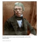
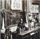
2。电光闪烁的物理世家 法拉第发现了:硫化银的导电性随温度上升而增加。一百多年后的今天,我们把它归纳到半导体的特性之一:热敏性。除了热敏性之外,半导体的特性还有:光敏性、整流性、以及掺杂性。这一节叙述‘光敏性’。 继法拉第之后,法国物理学家 A.E.贝克勒尔 Alexandre-EdmondBecquerel(1820–1891)发现了光生伏特效应。 http://www.medarus.org/Medecins/MedecinsTextes/becquerel.html 贝克勒尔一家四代五个物理学家,见上图。 A.E.贝克勒尔是中间一位,其余的是: AntoineCésar Becquerel (1788-1878), father of A.E.贝克勒尔。 LouisAlfred Becquerel (1814-1862), brother of A.E.贝克勒尔。 HenriBecquerel (1852-1908), son of A.E.贝克勒尔。 JeanBecquerel (1878-1953), grandson of A.E.贝克勒尔。 上图中的几个人,除了第二位贝克勒尔去世早,不广为人知,其余的都成就不凡。 A.E.贝克勒尔的父亲曾在拿破仑麾下服役,滑铁卢战役之后专攻科学,曾促进了电化学的创立,也是率先研究电发光现象的物理教授,A.E.贝克勒尔的儿子亨利·贝可勒尔,因发现天然放射性现象,与居里夫妇分享1903年的诺贝尔物理学奖。他的孙子后来也是法国颇负声名的物理学家。 我们现在知道,电和光都是能量的某种存在方式,这两种能量会互相转换。电转换成光的现象在大自然经常被观察到,比如:带电的大气放电时产生的闪电;科学家在研究放电现象时,也经常观察到的火花和闪光等。但是,从光到电的现象就不是那么普遍了。当时, A.E.贝克勒尔的父亲就是从化学的角度来研究电发光现象。老子研究从‘电’到‘光’,儿子则进一步地想,光是不是也能产生‘电’呢?果然不出所料,1839年,19岁的A.E.贝克勒尔在他父亲的实验室里,第一次观察到了这种现象。 A.E.贝克勒尔将氯化银放在酸性溶液中,用两片浸入电解质溶液的金属(铂)作为电极,见下图。贝克勒尔发现,如果有阳光照射时,两个电极间会产生额外的电压。这不就是‘光’转换成了‘电’吗?贝克勒尔将此现象称为光生伏特效应,这是历史上最早被发现的半导体的第二个特征。 贝克勒尔发现的是液体中的光生伏特效应,也被称为贝克勒尔效应。到 1883年,亚当斯等在金属和硒片上发现固态光伏效应,并制成了第一个“硒光电池” 【 1】 。 1873年,英国的史密斯发现硒晶体材料在光照下导电性增加,这是半导体又一个与光照有关的特性:光电导效应。 从现代物理学的观点,刚才所说的半导体的两个特性,和 1887年德国物理学家赫茲发现的光电效应,物理本质上是相关的,我们可把它们都归类于半导体的光敏性。也可以把它们统称为‘光电效应’。 光电效应 【 2】 最早是被德国物理学家赫茲发现的。赫茲用两个锌质小球做实验,当他用光线照射一个小球时,则发现有电火花跳过两个小球之间,如果用蓝光或紫外线照射,电火花最明显。这个现象后来( 1905年 )被爱因斯坦从量子力学的观点加以解释,使爱因斯坦得到 1921年的诺贝尔物理奖。 和贝克勒尔家庭类似,赫兹一家也有好几个物理学家。发现光电效应的海因里希·鲁道夫·赫兹( Heinrich Rudolf Hertz,1857-1894)和发现电磁波的赫兹是同一个人。鲁道夫·赫兹虽然只活了36岁,但他的两个发现都举足轻重:电磁波的发现证明了麦克斯韦电磁理论的正确性,而光电效应的发现对量子理论的创立及发展功不可没。 鲁道夫·赫兹的侄子古斯塔夫·路德维希·赫兹( Gustav Ludwig Hertz,1887年-1975年),也是物理学家,量子力学的先驱,1925年诺贝尔物理学奖获得者。路德维希·赫兹的儿子卡尔·赫尔穆特·赫兹(Carl Hellmuth Hertz , 1920-1990 )则发明了医疗用超声波技术和喷墨打印技术。 赫茲发现的是金属的光电效应,半导体也能产生光电效应,统而言之,光电效应指的是因光照而引起物体电学特性的改变。半导体的光电效应分为光电子发射、光电导效应和光生伏特效应。前一种发生在物体表面,又称外光电效应。后两种发生在物体内部,称为内光电效应。 半导体的光电效应 上图说明了几种光电效应的异同点。半导体材料无光照时,导带上有很少的自由电子。在光照射情况下,低能量的电子吸收了光子能量,从键合状态过度到自由状态。如果光子的能量足够大,使得电子能够逸出物质表面而发射出去,这便是被赫兹所观测到的光电发射效应,或称外光电效应。 如果低能级的电子吸收了光子能量后,并未被发射,而只是被激发跃迁到导带中,大大地增加了自由电子的数目,从而增强了物质的导电性。这种现象被称为:光电导效应。更进一步考虑,如果被光照射的物质材料是不均匀的,或由两种不同的物质层构成的情况。这时,由于两种物质在光照下产生的导电性能变化不一样,使得自由电子偏向于聚集到一种物质而离开另一种物质,由此而形成一个电位差,这便是 1839年首次被贝克勒尔观察到的光生伏特效应。 【 1】W.G. Adams andR.E. Day observed the photovoltaic effect in solidified selenium, and publisheda paper on the selenium cell. 'The action of light on selenium,' inProceedings of the Royal Society, A25, 113. 1877 【 2】Hertz, H.R.Ueber sehr schnelle electrische Schwingungen, Annalen der Physik,vol. 267, no. 7, p. 421-448, May 1887. http://matidavid.com/pioneer_files/Hertz.htm 上一篇:法拉第 系列科普目录 下一篇: 猫胡子侦测器
2012有机半导体国际研讨会.doc 2012 有机半导体国际研讨会邀请函 2012 年 6 月 3 日 至 6 月 4 日 湖南 长沙 尊敬的老师: 您好! 由国家自然科学基金委支持,中南大学主办的 2012 有机半导体国际研讨会( Organic Semiconductor Workshop 2012 )将于 6 月 3 日 至 4 日在湖南长沙举行 ,议题涵盖 有机发光二极管 ( OLED ) 、有机薄膜晶体管 ( OTFT ) 、有机太阳能电池 ( OPV ) ,有机半导体自旋电子学,有机半导体界面等。 有机半导体材料 (OSC) 近年来已发展为一类具有广阔应用前景的新型功能材料,积极开展对有机半导体材料及其器件的深入研究,对占领该领域的学科前沿和发展国民经济均具有重大的意义。此次国际研讨会邀请了众多国内外有机半导体领域的知名专家学者,旨在交流有机半导体最新进展和今后研究的发展方向,开展国内外同行间的合作,形成高水平的研究成果,提高研究生的培养水平,促进形成高水平的研究团队。 因此,我们诚挚地邀请您和您的同事及研究组成员拔冗光临研讨会并介绍工作成果。如能惠临,敬请使用附件 4 的会议回执,于 5 月 18 日以前发至 osc2012@csu.edu.cn 此致 敬礼! 2012 有机半导体国际研讨会组委会 2012 年 5 月 7 日 附件 1 2012 有机半导体国际研讨会日程和会务 一、会议日程: 1. 2012 年 6 月 2 日 ,嘉宾报到,现场注册。 2. 2012 年 6 月 3 日 ,开幕式、大会邀请报告。 3. 2012 年 6 月 4 日 ,大会邀请报告、各分会场小组专题报告。 4. 2012 年 6 月 5 至 6 日,张家界旅游 二、会务相关事项: 1. 报到地点:枫林宾馆(长沙市岳麓区枫林一路 43 号 ) 2. 会议注册:参加研讨会的注册费为人民币 800 元(研究人员)、 600 元(学生),住宿费、旅游费自理; 3. 大会语言:英语; 4. 墙报要求: 120CM *90CM ,请各位代表按要求自行打印并带至会场,按指定位置张贴; 5. 联系人:高永立(组委会主任 ) 邓宏贵(秘书长 13975159948 ) 张小姣(秘书 13973192264 ) Email: osc2012@csu.edu.cn 附件 2 :已应邀出席研讨会的主要嘉宾 已应邀出席研讨会的主要嘉宾 l 美国: Prof. Ching W. Tang, 美国工程院院士,罗切斯特大学教授,有机半导体发光二极管开创人, 2011 年 Wolf 奖得主; Prof. Franky So, 佛罗里达大学; Prof. Bin Hu, 田纳西大学 ; l 德国: Prof. Martin Aeschlimann, 德国凯泽斯劳滕大学教授,自旋分辨 - 时间分辨双光子能谱专家,德国物理学会表面分会主席; l 加拿大 : Prof. Zheng-Hong Lu, 多伦多大学,加拿大国家教授; l 日本: Prof. Nobuo Ueno; 千叶大学; l 新加坡: Prof. Wei Chen; 新加坡国立大学; l 香港: Prof. C.S. Lee, 香港城市大学,讲座教授 ; l 中国:曹镛院士, 华南理工大学;张泽院士,浙江大学;万立骏院士,中科院化学所;黄维院士,南京邮电大学;刘星元研究员,中科院长春光机所;邱勇教授、帅志刚教授,清华大学;闫东航研究员、马东阁研究员,中科院长春应化所; 廖良生教授,苏州大学;李永舫研究员,中科院化学所; 解士杰教授,山东大学 ; 吴镝教授,南京大学;中科院上海技术物理研究所,戴宁 附件 3 :会议日程总表 2012 有机半导体国际研讨会会议日程 时间 内容 参加人员 地点 6 月 2 日 全天 会议代表报到注册 全体代表 枫林宾馆 6 月 3 日 上午 大会开幕式 合影留念 大会邀请报告 全体代表 枫林宾馆 下午 大会邀请报告 全体代表 枫林宾馆 晚上 欢迎晚宴 全体代表 枫林宾馆 6 月 4 日 上午 大会邀请报告 全体代表 枫林宾馆 下午 小组专题报告 全体代表 中南大学 晚上 墙报及讨论 全体代表 中南大学 6 月 5-6 日 两天 会后考察 代表自愿参加 张家界 附件 4 :参会回执 2012 有机半导体国际研讨会参会回执 大会语言:英语 个人信息 姓 名 职务 / 职称 工作单位 联系电话 Email 报告及墙报情况 是否提供 题目 摘要(请包含题目、主要作者、单位及摘要主体内容。) 是否参加张家界旅游 备注: 1. 报告摘要及墙报内容请包含题目、主要作者、单位及摘要主体内容。 2. 参会住宿地点:枫林宾馆,请您填写住宿天数: 天 3. 回执请发至: osc2012@csu.edu.cn ; 4. 回执请您在 5 月 18 日前返回确认。 附近 5 :部分邀请报告情况 部分邀请报告情况 Invited Speakers Name Organization Country/Region Title Yong Cao South China University of Technology China WATER/ALCOHOL SOLUBLE CONJUGATED POLYMERS FOR INTERFACE MODIFICATION IN POLYMER BULK HETEROJUNCTION SOLAR CELLS Lijun Wan Institute of Chemistry, Chinese Academy of Sciences China Structural detail and property measurement of several typical organic molecule-based nanoarchitecture Ze Zhang Zhejiang University China No Zhigang Shuai Tsinghua University China Electron-phonon couplings in organic semiconductors So Franky University of Florida USA Carrier recombination in polymer solar cells Nobuo UENO Graduate SchoolofAdvancedIntegrationScience,ChibaUniversity Japan Unraveling mysteries in organic semiconductors: Charge mobility and energy level alignment Donghang Yan Changchun Institute of Applied Chemistry China Heterojunction effects and some applications in crystalline organic semiconductors Zhenghong Lu University of Toronto Germany Efficient Droop in OLED Liangsheng Liao Soochow University China Challenges of OLED Technology for Lighting Applications in China Ning Dai Shanghai Institute of Technical Physics, CAS China No Dongge Ma Sate Key Laboratory of Polymer Physics and Chemistry, Changchun Institute of Applied Chemistry, Chinese Academy of Sciences China High efficiency hybrid white OLEDs Shijie Xie School of Physics , Shandong University China Theoretical investigation on organic magnetoresistance based on hyperfine interaction Yongfang Li Institute of Chemistry, Chinese Academy of Sciences China Photovoltaic materials for high efficiency polymer solar cells Wei Chen National University of Singapore Singapore Epitaxial Graphene on SiC: Growth Mechanism and Surface Transfer Doping Xingyuan Liu State Key Laboratory of Luminescence and Applications , Changchun Institute of Optics, Fine Mechanics and Physics, Chinese Academy of Sciences China Electrically pumped organic semiconductor microcavity laser Lingling Wang Hunan University China Magnetic Edge-States in Chiral Graphene Nanoribbon with Reconstructed Edges
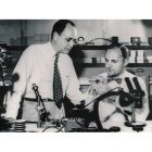
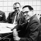
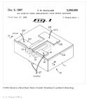
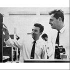
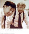
在 威廉 · 肖克利的PN结理论被验证 之后(1948年),制造 一个可以工作的结型晶体管仍然面临严峻的挑战。主要问题是缺乏足够纯净,均匀的半导体材料。贝尔实验室的化学家戈登 · 蒂尔认为,将需要大的单晶,锗和硅, 但听从的人很少,包括 肖克利 。 在管理层很少的支持下, 蒂尔建立自己所需的晶体生长设备, 在 机械工程师约翰小和欧内斯特 · 比埃勒技术员的帮助下。 他在 1917 年由波兰化学家 Jan Czochralski 开发的技术的基础上, 用 一个小的 “ 种子 ” 锗晶体在坩埚熔锗 中 慢慢地缩回来,形成一个狭长的单晶。 肖克利这一成就后来被称为 “ 在初期半导体领域最重要的科学 成果 。 采用这种技术,贝尔实验室的化学家 MorganSparks 通过在 熔融锗晶体生长过程中 加入 微小颗粒杂质,制作 pn 结。 在 1950 年 4 月,他和蒂尔开始向熔体中加入两个连续的小球,第一个是 p 型杂质和第二个是 n 型杂质,形成了内层很薄的 NPN 结构。 一年后,这种 “ 生长出的结型晶体管 ” 超越性能最好的点接触晶体管。 在 1951 年 7 月 4 日, 贝尔实验室在一次 会议 上宣布了这一发现,并强调了肖克利的贡献。 Gordon K. Teal(左)和Morgan Sparks在贝尔实验室,1951年 Morgan Sparks在1949年的第一个结晶体管 2006-2007 Alcatel-Lucent. All rights reserved 1951年,首批微瓦级面结型晶体管中的一只 2006-2007 Alcatel-Lucent. All rights reserve 贝尔M1752型商用结晶体管,约在1951年 Courtesy of: Jack Ward - Transistor Museum 译者:哈尔滨工业大学(威海)电子封装 090840111-计孝智 校对:哈尔滨工业大学(威海)电子封装 090840114-刘继伟 版权 copyright by www.nobeprize.org 原文: http://www.computerhistory.org/semiconductor/timeline/1951-First.html After William Shockley’s theories about p-n junctions had been validated by tests ( 1948 Milestone ), fabricating a working junction transistor still presented formidable challenges. The main problem was lack of sufficiently pure, uniform semiconductor materials. Bell Labs chemist Gordon Teal argued that large, single crystals of germanium and silicon would be required, but few - including Shockley - were listening. With little support from management, Teal built the needed crystal-growing equipment himself, with help from mechanical engineer John Little and technician Ernest Buehler. Based on techniques developed in 1917 by the Polish chemist Jan Czochralski, he suspended a small "seed" crystal of germanium in a crucible of molten germanium and slowly withdrew it, forming a long, narrow, single crystal. Shockley later called this achievement "the most important scientific development in the semiconductor field in the early days." Employing this technique, Bell Labs chemist Morgan Sparks fabricated p-n junctions by dropping tiny pellets of impurities into the molten germanium during the crystal-growing process. In April 1950, he and Teal began adding two successive pellets into the melt, the first with a p- type impurity and the second n- type, forming n-p-n structures with a thin inner, or base, layer. A year later, such “grown-junction transistors” surpassed the best point-contact transistors in performance. Bell Labs announced this advance on July 4, 1951 in a press conference featuring Shockley.
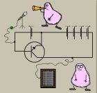
在放大的情况下,晶体管用于放大信号,如声音信号的放大。左边是一个用来放大声音信号的电路的例子。进入麦克风的声音被转换成电信号,这个信号在晶体管中被放大。然后这个被放大的声音信号通过电路,直到它到达扬声器。扬声器将这个声音的电信号重新转换成声音。从音箱中发出的声音与进入麦克风的声音是完全相同的,只是更加响亮了。这就是所谓的放大 - 声音被放大了。 译者:哈尔滨工业大学(威海)电子封装 090840228-谢战胜 校对:哈尔滨工业大学(威海)电子封装 090330112-张慧颖 http://www.computerhistory.org/semiconductor/timeline/ Amplification .html Amplification In the case of amplification the transistor is used to amplify a signal. One example of such a signal can be a sound. To the left is an example of a circuit that is used to amplify sound signals. The sound entering the microphone is converted to an electrical signal that is amplified in the transistor. This amplified sound signal then travels through the circuit until it reaches the loudspeaker. This speaker converts the electrical sound signal back into a sound. The sound leaving the speaker is the same as the sound that entered the microphone, only much louder. This is called amplification – the sound is being amplified. 版权 copyright by www.nobeprize.org 放大
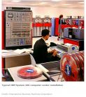
半导体里程 _ 博物馆 _1966- 半导体读写存储器 1966 年 , 半导体读写存储器适用于满足高速存储的需要。因为拥有高性能的存储区和高速缓存的应用,双极性的 RAM 开始进入计算机市场 随机读写存储器储存信息变化频繁因此必须快速存取。到 20 世纪 70 年代中期,由于具有最低的单位存储位成本,磁性铁氧体磁芯阵列占据了随机存储技术的主导地位。 1963 年, Robert Norman 在仙童半导体公司研发取得了半导体静态 RAM 的设计专利。在 1965 年, Scientific Data Systems, Santa Monica, CA and Signetics 几家公司合作开发出了一种全解码的 8 位双极型器件,并且在同年晚些时候元器件工程师 Ben Agusta and Paul Castrucci 开发出了 SP95 ——一种用于 IBM 系统的 16 位的 RAM 。 1966 年, Tom Longo 领导的团队为霍尼韦尔公司 4200 型小型计算机设计的 16 位晶体管逻辑电路高速暂存存储器 TMC3162 成为第一个被广泛使用的半导体 RAM 。仙童公司、西尔瓦尼亚公司、美国德州仪器公司也开始制造这种产品。随后产生的 64 位器件有以下几种: IBM 的缓存芯片、仙童公司的 9035 和 93403 ,因特尔的 3101 ,和德州仪器的 SN7489. 1969 年, IBM 纽约州东费西基尔研究中心为 1971 的装运系统生产出了 128 位的器件—— 370 Model 145 ,这是该公司的第一个商业计算机采用的半导体主存储器。 1970 年 4 月,仙童公司使用 H.T. Chua 设计的 256 位晶体管逻辑电路芯片 4100 ( aka93400 )完成了为宝来公司 Illiac IV 设计的半导体主存储系统。使用 Douglas Peltzer’s Isoplanar 的脱氧过程,能够在提高速度的同时减少硅片的消耗。 1971 年, Bill Herndon 据此设计出了一种快速的 256 位晶体管逻辑电路存储器 93410 。以 Isoplanar 过程为基础,克雷一号超级计算机使用了 65000 个仙童公司生产的 1024 位 ECL RAM 。双极性技术能让计算机速度更快,但是它需要使用 MOS 程序来推广低成本的解决方案以便于主存储器得到广泛的多用途的应用。 译者 : 哈尔滨工业大学 ( 威海 )090840212 高丙欢 校对 : 哈尔滨工业大学 ( 威海 )090840213 邱东阳 http://www.computerhistory.org/semiconductor/timeline/1978- Semiconductor .html 版权 copyright by www.computerhistory.org Metal mask plot for a 16-bit bipolar TTL RAM. Screen image from a 1967 TV documentary 具有16位双极性晶体管逻辑电路读写存储器的金属掩膜图片 拍摄于一部1967年的电视纪录片 128-bit bipolar RAM designed for the IBM System/360 Model 145 main memory is compared to a magnetic core array 为IBM系统设计的128位双极性RAM,主存储器是磁芯阵列 256-bit TTL RAM used in the Illiac IV Processor Element Memory 256位晶体管逻辑电路RAMIlliac IV处理机器件存储器中使用的256位晶体管逻辑电路RAM The Cray 1 supercomputer used 65,000 Fairchild 10415 high-speed 1024-bit ECL chips for main memory 主存储器中含有65000个仙童公司生产的高速1024位ECL芯片 英文原文 1966 - Semiconductor RAMs Serve High-speed Storage Needs Bipolar RAMs enter the computer market for high-performance scratchpad and cache memory applications. Credit: Fairchild Camera Instrument Corporation Random Access Read-Write Memories (RAMs) store information that changes frequently and must be accessed quickly. Offering the lowest cost per storage bit, magnetic ferrite core arrays comprised the dominant RAM technology through the mid-1970s. Robert Norman patented a semiconductor static RAM design at Fairchild in 1963 that was later used by IBM as the Harper cell. In 1965 a cooperative development between Scientific Data Systems , Santa Monica, CA and Signetics produced a fully-decoded 8-bit bipolar device and later that year Components Division engineers Ben Agusta and Paul Castrucci developed the SP95, a 16-bit RAM for the IBM System /360 Model 95 . A team led by Tom Longo at Transitron built the TMC3162 16-bit TTL scratchpad memory for the Honeywell Model 4200 minicomputer in 1966 that became the first widely second sourced semiconductor RAM. Fairchild (9033), Sylvania (SM-80), and TI (SN7481) also manufactured the design. 64-bit devices followed from IBM (cache memory chip), Fairchild (9035 and 93403), Intel (3101), and TI (SN7489) In 1969 the IBM East Fishkill, NY facility produced a 128-bit device for the 1971 shipment of System/370 Model 145, the company's first commercial computer to employ semiconductor main memory. Using the 4100 (aka 93400) 256-bit TTL chip designed by H.T. Chua, Fairchild delivered semiconductor main memory systems for the Burroughs Illiac IV computer in April 1970. Using Douglas Peltzer’s Isoplanar oxide-isolated process that improved speed while consuming less silicon area, Fairchild's Bill Herndon designed a fast 256-bit TTL memory (93410) in 1971. The Cray 1 supercomputer introduced in 1976 used 65,000 Fairchild 1024-bit ECL RAM chips (10415) based on the Isoplanar process Bipolar technology enabled faster computers but it took the MOS process to deliver low-cost solutions for widespread use in main memory and general-purpose applications. ( 1970 Milestone )
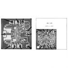
IBM的工程师们开发了用以减少研发错误和设计时间的计算机辅助电子设计自动化工具。 当集成电路开始包含几百个门电路和数以千计的晶体管时,他们所支持的计算机已经可以完成加快设计速度和减少设计错误的任务了。这个方法被称作 CAD (计算机辅助设计)或者 EDA (电子设计自动化)。 IBM 在 20 世纪 50 年代末率先开发了在 700 系列电脑文档下运行的 EDA 程序。到了 1966 年, James Koford 和他的同事们在 IBM 纽约州东费西基尔公司用图形显示器采集 STL 混合电路模块( 1964 里程碑事件)的图案,检查他们的错误并自动将信息转换为掩膜模式。在 Koford 加入 Fairchild RD 后他又与 Hugh Mays 、 Ed Jones 及其他同事一起将这项程序应用于单片集成电路。他们的努力创造了逻辑模拟软件( FAIRSIM )、测试程序生成器软件以及门列阵和标准单元布局布线软件( 1967 年里程碑事件),这些为一代又一代的 EDA 工具打下了坚实的基础。 EDA 有两个重要项目源于非主流产业。 20 世纪 60 年代, Larry Nagel 和 Donald Pederson 以及后来的贡献者 Richard Newton 在美国加州大学伯克利分校开发了 SPICE (模拟集成电路重点项目)电路仿真程序。 1979 年,加州理工学院的 Lynn Conway of Xerox 和 Carver Mead 在他们论著的《超大规模集成电路系统导论》中描述的一个新方法揭开了系统设计和芯片设计过程秘密。 20 世纪 80 年代,益华电脑和美国新思科技公司受到在柏克莱加州大学( SIS )、洛杉矶加利福尼亚大学( RSAP )和科罗拉多大学( BOLD )所做调查的激发,开始对综合逻辑系统进行商业化的包装。这些和先进的布局布线技术、逻辑模拟技术以及其他厂商已有的设计核查规则共同使集成电路的设计生产能力能够紧跟设备复杂度不断增加的步伐。 IBM 360/67 仙童公司 1967 年的以大型计算机为运算动力的 CAD 设计系统 图 1 编辑者:费尔柴尔德摄像机仪器公司 掩模草图数字化手绘系统工具 图 2 提供者:因特尔公司 20 世纪 80 年代基于集成电路 CAD 设计系统的工作站 图 3 米德和加威的成就获得了 1981 年的美国电子奖 图 4 译者:哈尔滨工业大学(威海)电子封装 090840213- 邱东阳 校对:哈尔滨工业大学(威海)电子封装 090840229-朱泯西 版权 copyright by www.computerhistory.org 1966 - Computer Aided Design Tools Developed for ICs IBM engineers pioneer computer-aided electronic design automation tools for reducing errors and speeding design time. IBM 360/67 mainframe-powered CAD system at Fairchild in 1967 Credit: Fairchild Camera Instrument Corporation Mask layout drawing hand digitizing system tool Courtesy of: Intel Corporation Workstation-based integrated circuit CAD system 1980s 1981 Electronics Award for Achievement to Conway and Mead As ICs began to incorporate hundreds of gates and thousands of transistors, the computers they enabled were harnessed to speed the design task and eliminate errors. This process is called CAD (Computer Aided Design) or EDA (Electronic Design Automation). IBM pioneered EDA in the late 1950s with documentation of the 700 series computers. By 1966 James Koford and his colleagues at IBM Fishkill were capturing SLT hybrid circuit module ( 1964 Milestone ) designs on graphical displays, checking them for errors and automatically converting the information into mask patterns. After Koford joined Fairchild RD he worked with Hugh Mays, Ed Jones, and others to apply this process to monolithic ICs. Their efforts created logic simulators (FAIRSIM), test program generators, and place and route software for gate arrays and standard cells ( 1967 Milestone ) that laid the ground work for generations of EDA tools. Two important EDA projects originated outside the mainstream of the industry. Larry Nagel and Donald Pederson, with later contributions by Richard Newton, at U.C. Berkeley developed the SPICE (Simulation Program with IC Emphasis) circuit simulation program in the 1960s. A new methodology described in the 1979 Introduction to VLSI Systems by Lynn Conway of Xerox, PARC and Carver Mead of California Institute of Technology demystified the process of chip design for system designers. Commercial logic synthesis packages from Cadence and Synopsys in the 1980s were stimulated by research at U.C. Berkeley (SIS), U.C.L.A. (RASP), and University of Colorado, Boulder (BOLD). These, together with advancements in place and route, logic simulation, and design rule verification from other vendors, allowed IC design productivity to keep pace with increasing device complexity.
第三方供应商发展到具备了半导体结构的专业知识,并且作为技术改进的及关键部分生产设备的供应商出现。 在半导体工业发展的第一个十年,行业推行了 5 种基本结构的晶体管:点接触式晶体管、生长结式晶体管、合金结式晶体管、表面势垒式晶体管和扩散底层式晶体管。 制造商架构起他们自己的生产设施设备投入到每一代产品的制造中。杰克 ·基尔比( 1958 年里程碑式人物)注意到说:“可能我们用到的设备的最贵的那一部分要花费至少 1 万美金 。 由于产品通过平面法( 1959 年的里程碑)向大型化发展,因此出现了产业的和独立的设备制造商,从而将工艺技术也标准化了。制造商专门研究了前端(晶圆加工)和后端(封装、组配和测试)( 1961 年的里程碑)的生产运行。 前端的生产设备,随着晶圆尺寸从 1958 年的 0.5 英寸增大到今天的 12 英寸( 300mm ),其价格也呈数量级增长。早期的前端的生产设备配套供应商包括赛默公司(扩散熔炉)和它旗下的日本电子有限公司、 DW 工业(沉积系统),以及 GCA Mann 和铂金埃尔默公司(光刻设备)( 1955 年的里程碑)。伊智公司, 1961 年费雅嘉分拆出的一个子公司,生产建造了用于晶圆测试的探测设备。 瓦里安公司建造了蒸发器、真空泵和离子注入系统。成立于 1967 年,为制造外延薄膜( 1960 年的里程碑)提供化学气相沉积系统的应用材料公司,通过鼓励半导体供应商将其对制造工艺开发发展工作转交给他们的设备供应商,从而给行业动向带来了改变。 技术工艺的第三方资源,使半导体公司得以关注产品的体系结构及应用,而不再关注于生产和制造工艺的专业知识。这就造成了晶圆代工工厂的兴起,在 19 世纪 80 年代,这些工厂支持了作为新类型的无晶半导体公司的发展。 译者:哈尔滨工业大学(威海)电子封装 090840214葛峰 校对:哈尔滨工业大学(威海)电子封装 090840215申聪敏 原文: http://www.computerhistory.org/semiconductor/timeline/1967-Equipment.html 版权 copyright by www.computerhistory.org 1967 - Turnkey Equipment Suppliers Change Industry Dynamics Third-party vendors develop specialized knowledge of semiconductor fabrication and emerge as vendors of process technology and turnkey manufacturing facilities. During its first decade the semiconductor industry went through five basic transistor structures: point contact, grown junction, alloyed junction, surface barrier, and diffused-base. Manufacturers built their own equipment to support each generation. Jack Kilby ( 1958 Milestone ) noted that "probably the most expensive piece of equipment that we used cost less than $10,000." As production moved to high volumes with the planar process ( 1959 Milestone ), techniques were standardized across the industry and independent equipment producers emerged. Vendors specialized in "Front End" (wafer processing) or “Back End” (package, assembly, and test) ( 1961 Milestone ) operations. Front-end equipment prices increased by orders of magnitude as wafer diameters grew from 0.5 inches in 1958 to today’s 12 inches (300mm). Early front-end tool suppliers include Thermco (diffusion furnaces) and its Japanese licensee Tokyo Electron Ltd, DW Industries (deposition systems), and GCA/Mann and Perkin Elmer (photolithography) ( 1955 Milestone ).Electroglas, a 1961 Fairchild spinout, built probe equipment for wafer testing. In 1965 Kulicke Soffa introduced commercial contact aligners. Varian Associates built evaporators, vacuum pumps, and ion-implantation systems. Founded in 1967 to supply chemical vapor deposition systems for epitaxial films ( 1960 Milestone ), Applied Materials initiated a change in industry dynamics by encouraging semiconductor vendors to shift responsibility for development of manufacturing technology to their equipment suppliers.Third-party sources of technology allowed the semiconductor companies to focus on product architecture and applications rather than process and manufacturing expertise. This led to the rise of "wafer-foundry" vendors who supported a new breed of "fabless" semiconductor companies in the 1980. Michael McNeilly Walter Benzing pioneered epitaxial deposition equipment at Applied Materials, Inc. (应用材料公司倡导外延沉积设备的先驱——迈克尔 ·麦克尼尔,沃尔特·本辛 ) Credit : Semiconductor Equipment and Materials International (SEMI) Applied Materials Model AMV 800 chemical vapor deposition epitaxial reactor (1969) (应用材料公司化学气相沉积外延反应设备 AMV 800 模型) Credit : Applied Materials Technology, Inc Electroglas Model 131B Motorized/Manual Prober allowed testing of die on the wafer before packaging (伊智公司的用于测试封装前晶圆上芯片的自动 / 手动探测器 131B 模型) Credit : Electroglas, Inc Perkin Elmer Micralign projection mask aligner team 1973 ( 1973 年铂金埃尔默公司的 Micralign 投射掩膜对准器团队) Credit : Semiconductor Equipment and Materials International (SEMI)
用自动化设计工具减少开发工程的时间和设计,并提供复杂的定制集成电路 随着英特网共享连接变得复杂化,他们的设计和生产周期延伸到好几年,而一些最终产品寿命周期缩短到一个季度。 1967 年,为了加快美国空军大批量复合定制电路的生产速度, IBM 和德州仪器开发了 “ 自行分配 布线 ” 的方法,采用唯一的一台计算机生成( 1966 年里程碑)每个晶圆金属掩模的技术。 为量产定制设计开发的两种方法是门阵列和标准单元 。他们统称为特定应用集成电路( ASIC )。门阵列是无连接的晶体管的晶片片生产技术。最终定制互连技术确定为最后的生产方案,虽然它比手工制作芯片的硅使用效率低,但是雏形可以从几个月的生产周期缩短为几天。早期门阵列供应商,如费伦蒂 / 协调会是手工的定制连接。 1967 年,飞兆半导体公司在推出微矩阵系列——双极 DTL 和 TTL 电阵列,此阵列可用 CAD 工具来执行两者的相互操作。 1974 年, 罗伯特·利普为国际集成电路设计了第一款 CMOS 阵列,但是可行的 CAD 支持在若干年后也没人设计出来。 标准单元的英特尔网络共享连接采用了一系列应用了装配目录功能设计的制造板罩,并存储在电脑存储信息库中。 他们提供了一个硅高效的手工设计和门阵列的快速掉头之间的折中的方法。 飞兆半导体和摩托罗拉提供的一个早期的 MOS 标准单元权限低于商品牌号 Miscromosaic 和 Polycell 。 超大规模集成电路技术(成立于 1979 年)和 LSI Logic ( 1981 )成功地利用 20 世纪 70 年代被遗弃的 CAD 为基础的 ASIC 概念。当时被摒弃就是因为花费大量的计算时间。 Fairchild 4500 - a 1967 DTL 32-gate Micromatrix custom array designed using CAD tools to interconnect two layers of metal 飞兆半导体 4500 - 1967 年 DTL32 门的 Micromatrix 自定义数组使用 CAD 工具设计,两层金属互连 Credit: Fairchild Camera Instrument Corporation Micromosaic - a 1968 standard cell design for GE Avionics. One of the industry's first designs for revenue micromosaic - 1968 年为 GE 航空电子标准电池的设计。一个行业的第一个设计收入 Credit: Fairchild Camera Instrument Corporation IBM LSI MOD1, an experimental discretionary-wired wafer design by IBM fabricated by Texas Instuments IBM LSI MOD1 , 由 IBM 酌情 - 连接的实验晶片设计由德州自控制作 Credit: International Business Machines Corporation A Ferranti ULA (Uncommitted Logic Array) integrated 14 TTL IC packages for the Sinclair ZX81 PC in 1981 一个费伦蒂 ULA (自由逻辑阵列)集成了 14 组 TTL IC 封装 在 1981 年辛克莱 ZX81 PC Credit: Sinclair Research 1967 - Application Specific Integrated Circuits employ Computer-Aided Design Automated design tools reduce the development engineering time to design and deliver complex custom integrated circuits. As ICs increased in complexity their design and manufacturing turn-around times stretched out to years even as some end product life cycles shrank to a single season. To speed the availability of prototype quantities of complex custom circuits for the Air Force in 1967 IBM and Texas Instruments developed “discretionary-wiring” approaches that employed a unique computer-generated ( 1966 Milestone ) metal mask for every wafer.Two approaches developed for volume production of custom designs are gate arrays and standard cells - collectively known as Application-Specific ICs (ASIC). Gate arrays are produced as wafers of unconnected transistors. As the customizing interconnections are applied at the final manufacturing step, although less efficient in silicon usage than handcrafted chips, prototypes can be produced in days rather than months. Early gate array suppliers such as Ferranti/Interdesign designed the custom connections manually. In 1967 Fairchild introduced the Micromatrix family of bipolar DTL and TTL arrays that used CAD tools to perform this operation interactively. Robert Lipp designed the first CMOS array for International Microcircuits in 1974 but viable CAD support was not forthcoming for several years. Standard cell ICs employ a full set of fabrication masks using designs assembled from catalog functions stored in a computer library.They offer a compromise between silicon-efficient handcrafted designs and the fast turn-around of gate arrays.Fairchild and Motorola offered early MOS standard cell capabilities under the trade names Micromosaic and Polycell. VLSI Technology (founded 1979) and LSI Logic (1981) successfully exploited these CAD-based ASIC concepts abandoned by the original vendors in early 1970s largely due to the then high cost of computing time. 译者:哈尔滨工业大学(威海)电子封装 090840215 申聪敏 校对:哈尔滨工业大学(威海)电子封装 090840214 葛峰 原文: http://www.computerhistory.org/semiconductor/timeline/1967-ASICs.html 版权: copyright by www.computerhistory.org
Jack Kilby 图一 杰克 基尔比 Robert Noyce 图二 罗伯特 诺伊斯 一个集成电路由一个单片半导体材料制成,除了晶体管,还包含其他电子元器件。集成电路的发明者是杰克 基尔比和罗伯特 诺伊斯,而罗伯特 诺伊斯去世于1990年。杰克 基尔比于2000年获得了诺贝尔物理学奖。 译者:哈尔滨工业大学(威海)电子封装 070810427-苏琬茹 校对: 原文: http://www.nobelprize.org/educational/physics/transistor/function/ic.html 版权 copyright by www.nobeprize.org ———————————————————————————————— An integrated circuit is made of a single piece of semiconductor material and contains, apart from transistors, other electronical components. The inventors of the integrated circuit were Jack Kilby and Robert Noyce who died in 1990. Jack Kilby was awarded the Nobel Prize in Physics 2000.
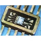
1958- 硅台面晶体管进入商业生产 飞兆半导体 生产双扩散硅台面晶体管满足苛刻的航空航天应用 1958 年初,仙童半导体公司以 150 美元从美国联邦系统分部采购 100 晶体管的第一笔订单。 没有既定的生产能满足其 严格规范的 70 车载电脑带有 高压硅晶体管驱动磁芯存储器 。随着 2 个发展项目的推行。戈登穆尔领导的一个小组和吉恩 · 赫尔尼在 pnp 装置中开发了一个 NPN 晶体管和吉恩 · 赫尔尼。 在短短的五个月,创始人(谢尔登罗伯茨)建立的晶形操作( 1956 关),发展光刻掩模技术,使用 16 毫米 movie-camera 镜头(罗伯特诺伊斯),建立了铝所需的特点,为使电气接触(穆尔),并建有自己的生产和试验设备(尤利乌斯空白,胜利格里尼奇,尤金克莱纳)在帕洛阿尔托设施。建筑在暴露于贝尔实验室技术( 1954 关)在肖克利,他们开发了第一个商用双扩散(发射器和基地)硅晶体管,所以命名为其提出的高原样结构。成功后交付的穆尔队的 NPN 晶体管的装置,在 1958 八月介绍了 2n697 型大获好评的惠施康贸易展。 自动控制学为选定的设备使应用在拦截导弹的导航控制系统成为这领域最强的防御。在 1958 年底,一个潜在的可靠性问题使新公司的生存岌岌可危。在金属封装中剥落的微小颗粒对短跨暴露交界处的台地结构产生威胁。 hoerni 的解决方案,著名的平面工艺( 1959 关),彻底改变了工业覆盖暴露有二氧化硅的交界处。 lobby, circa 1960 “ 仙童八 ” 创始人的姿势在公司的大厅,大约 1960 Courtesy of: Wayne Miller, Magnum Photos A B-70 supersonic bomber takes off Credit: U. S. Air Force 70 超音速轰炸机起飞 Fairchild Semiconductor wafer diffusion area, Palo Alto, circa 1958 Credit: Fairchild Camera and Instrument Corporation 飞兆半导体晶 片扩散面积,帕洛阿尔托,大 Detail of a Minuteman I guidance computer Credit: CHM Collection. Gift of Aron Insinga 详细的民兵我制导计算机 译者:哈尔滨工业大学(威海)电子封装 090840122-王孝宝 校对: 王天卓090840121 http://www.computerhistory.org/semiconductor/timeline/1978-PAL.html (原文) 版权 copyright by www.computerhistory.org ———————————————————————————————————— 滨工业大学(威海) 1958 - Silicon Mesa Transistors Enter Commercial Production Fairchild Semiconductor produces double-diffused silicon mesa transistors to meet demanding aerospace applications. In early 1958 Fairchild Semiconductor procured its first order, for 100 transistors at $150 apiece from IBM’s Federal Systems Division. No established manufacturer could meet its exacting specifications for a high-voltage silicon transistor to drive magnetic core memory in the B-70 on-board computer. Two development projects were pursued in parallel. A team led by Gordon Moore developed an n-p-n transistor and by Jean Hoerni, which worked on a p-n-p device. In just five months, the founders ( 1956 Milestone ) set up a crystal-growing operation (Sheldon Roberts), developed photolithographic masking techniques using 16 mm movie-camera lenses (Jay Last, Robert Noyce), established the aluminum characteristics needed for making electrical contacts (Moore), and built their own manufacturing and test equipment (Julius Blank, Victor Grinich, Eugene Kleiner) at their Palo Alto facility. Building on their exposure to Bell Labs techniques ( 1954 Milestone ) at Shockley, they developed the first commercial double-diffused (emitter and base) silicon mesa transistor, so named for its raised plateau-like structure. After successful delivery of the Moore team's n-p-n transistor, the device was introduced as type 2N697 to great acclaim at the Wescon trade show in August 1958. Autonetics selected the device for a guidance-and-control system on the Minuteman ballistic missile, the largest defense program of the era. In late 1958 a potential reliability problem put the new firm’s survival at stake. Tiny particles flaking off the inside of the metal package threatened to short across exposed junctions on the mesa structure. Hoerni's solution, the famous planar process ( 1959 Milestone ), revolutionized the industry by covering the exposed junction with silicon dioxide.
1956- 硅片在硅谷首次出现 肖克利半导体实验室 建造了 加州北部的第一个原型开发半导体设备 来为 硅谷训练年轻的工程师和科学家 。 1955 年 9 月 , 威廉萧克利和阿诺贝克曼同意 建立肖克利半导体实验室作为贝克曼的部门来“积极 、大力开展 关于半导体材料的 活动 ”。肖克利在加利福尼亚州山景城 圣安东尼奥南部道路 租用了 391 号楼,同时,开始招聘“世界上 最有创造力的团队开发、设计、生产晶体管 ”。 他吸引了很 多 能干的工程师和科学家 ,其中 了解和开发硅相关技术和工艺 、 扩散 技术的 戈登 · 摩尔和罗伯特 · 伊斯 都被他招聘来工作。 1956 年 12 月萧克利 因为 发明晶体管获得了诺贝尔物理学奖 ,但是,他的助理开始厌倦了他懒散的管理模式。 他们也觉得公司应该追求更直接生产硅晶体管的机会 而不是期盼遥远的目标“他在实验室将硅应用到电话通讯领域”。 在要求肖克利再雇用一名新的管理后, 摩尔 、 尤利乌斯 · 伊斯 、 格里尼克 、 琼 · 霍尔尼 、 克莱纳 、 拉斯特 、 罗伯茨 8 名 萧克利员工 在 1957 年 9 月 辞职并创立了 美国飞兆半导体公司 在 帕洛阿尔托 。 许多 来自 播实之星的员工 随之而来。 在未来十年 里, 快捷半导体 成长为 在半导体产业最重要的和创新的公司 ,引导了硅谷其他企业科技和文化,其中超微半导体和 英特尔 连接技术,但是,他的公司从来没有获得实际的利润。 贝克曼 在 1960 年 把专利卖给了 Clevite 公司 。 萧克利在斯坦福大学成了一个教授的电气工程与应用科学 的老师。 Toasting Shockley's Nobel Prize award at Rickey's Hotel, Palo Alto, CA. Celebrants include G. Moore, S. Roberts, R. Noyce, and J. Last 肖克利诺贝尔奖奖在里奇的酒店,帕洛阿尔托约礼,包括穆尔,罗伯茨,诺伊斯,和 J · The Shockley Semiconductor Laboratory facility, Mountain View, CA. circa 1960. 肖克利半导体实验室设施,山景,约公元 1960 。 Small-scale silicon zone refining in the Shockley laboratory in Mountain View 小型硅精炼的肖克利实验室在山景 Small-scale silicon zone refining in the Shockley laboratory in Mountain View 小型硅精炼的肖克利实验室在山景 1956 - Silicon Comes to Silicon Valley Shockley Semiconductor Laboratory develops Northern California's first prototype silicon devices while training young engineers and scientists for the future Silicon Valley. In September 1955 William Shockley and Arnold Beckman agreed to found the Shockley Semiconductor Laboratory as a Division of Beckman Instruments "to engage promptly and vigorously in activities related to semiconductors." Shockley rented a building at 391 South San Antonio Road in Mountain View, California, and began recruiting "the most creative team in the world for developing and producing transistors." He attracted extremely capable engineers and scientists, including Gordon Moore and Robert Noyce, who learned about and developed technologies and processes related to silicon and diffusion while working there. In December 1956 Shockley shared the Nobel Prize in Physics for inventing the transistor, but his staff was becoming disenchanted with his difficult management style. They also felt the company should pursue more immediate opportunities for producing silicon transistors rather than the distant promise of a challenging four-layer p-n-p-n diode he had conceived at Bell Labs for telephone switching applications. After unsuccessfully asking Beckman to hire a new manager, eight Shockley employees - including Moore and Noyce plus Julius Blank, Victor Grinich, Jean Hoerni, Eugene Kleiner, Jay Last and Sheldon Roberts - resigned in September 1957 and founded the Fairchild Semiconductor Corporation in Palo Alto. Many other employees, from technicians to PhDs, soon followed. Over the next decade, Fairchild grew into of the most important and innovative companies in the semiconductor industry, laying the technological and cultural foundations of Silicon Valley while spinning off dozens of new high-tech start-ups, including Advanced Micro Devices (AMD) and Intel. Shockley continued pursuing his four-layer diode but his company never realized a profit. Beckman sold the operation to Clevite Corporation in 1960. Shockley became a professor of electrical engineering and applied science at Stanford University. 译者:哈尔滨工业大学(威海)电子封装 090840120-王开伟 校对:哈尔滨工业大学(威海)电子封装 090840117-康志龙
1954 ——硅晶体管提供优越的工作特性 Morris Tanenbaum 在贝尔实验室制造出第一个晶体管,但是第一个把它应用于商业设备制做和销售的是德州仪器的工程师们。 在晶体管存在的前六年,他们一般都是由锗制造出来的。 虽然此元素是比硅更容易得到,并且它支持允许更高频率的操作,但是用它制成的固体器件,在“关”状态下泄漏电流有很大缺陷——那简直是对计算机逻辑的诅咒。 它们也仅限于 0 至 70 ° C 的操作,这也限制了它们在特殊应用程序下的使用。在 杜邦公司开始提供高纯度的半导体级硅材料后,硅器件在 -55 到 125 ° C 条件下使用成为可能 。 在 1954 年 1 月,贝尔实验室的化学家 Morris Tanenbaum 使用摩根·斯巴克斯和戈登·蒂尔的成长交界技术的变化,塑造了第一个硅晶体管。 但是实验室没有在追求它的进一步发展,思考它在商业化生产中的吸引力,这使得几个月后德州仪器( TI )将这一突破性的成果收入囊中。 蒂尔聘请了一队科学家和工程师,离开贝尔实验室在 TI 的组织实验室,由化学家威利斯阿德科克领导研究的硅晶体管。他们采用高纯度杜邦硅,他们的第一个成功的硅晶体管于 1954 年 4 月 14 日制作出来 —— 一个 NPN 结构使用成长结技术。 Tanenbaum 的研究没有了解到的,在 5 月 10 日,俄亥俄州代顿的无线电工程师学会会议提出这一成就,蒂尔由宣布硅晶体管的生产和可供出售创造一个轰动。在 几乎没有竞争的情况下, TI 占据了未来几年的硅晶体管的市场,并取得重大进展直到雷神公司的地位达到成为为世界上最大的商业晶体管的市场供应商。到 20 世纪 50 年代末,硅已成为业界首选的半导体材料。 图一 1954年5月莫顿琼斯的设计出了TI的第一个晶体管的略图 Morton Jones’s May 1954 design sketch of TI's first silicon transistor 图二 1954 TI的 硅晶体团队成员:w .Adcock,mM. Jones, E. Jackson, and J. Thornhill TI's 1954 silicon-transistor team: W. Adcock, M. Jones, E. Jackson, and J. Thornhill 图三 德州仪器公司做的广告强调硅晶体管体积小 Texas Instruments silicon transistor advertising emphasizes small size 图四 莫里斯高(左)与查尔斯丠(右)在贝尔实研室 Morris Tanenbaum (left) and Charles Lee (right) at Bell Labs 译者:哈尔滨工业大学(威海)电子封装 090840116-赵英建 校对:哈尔滨工业大学(威海)电子封装 090840115-刘金鑫 原文 http://www.computerhistory.org/semiconductor/timeline/1954-Silicon.html 版权: 2007 Computer History Museum. All rights reserved. 1401 N. Shoreline Blvd., Mountain View CA 94043 Ph 650-810-1010 ———————————————————————————————— 1954 - Silicon Transistors Offer Superior Operating Characteristics Morris Tanenbaum fabricates the first silicon transistor at Bell Labs but Texas Instruments' engineers build and market the first commercial devices. For the first six years of their existence, transistors had all been made with germanium. Although this element is much easier to work with than silicon and allows higher-frequency operation, solid-state devices made with it have far worse leakage currents in the "off" condition - an anathema for computer logic. They are also restricted to 0 to 70°C operation, which limits their use in rugged applications. Silicon devices that function from -55 to 125°C became possible after Dupont began supplying high-purity "semiconductor-grade" material. In January 1954 Bell Labs chemist Morris Tanenbaum fashioned the first silicon transistor using a variation on Morgan Sparks and Gordon Teal’s grown-junction technique. But the Labs did not pursue the process further, thinking it unattractive for commercial production, which allowed Texas Instruments (TI) to claim credit for this breakthrough several months later. Having left Bell Labs to organize a research lab at TI, Teal hired a team of scientists and engineers led by chemist Willis Adcock to work on silicon transistors. Employing high-purity Dupont silicon, they made their first successful silicon transistor — an n-p-n structure using the grown-junction technique — on April 14, 1954. Unaware of Tanenbaum’s work, Teal presented this achievement on May 10 at an Institute of Radio Engineers conference in Dayton, Ohio, creating a sensation by announcing that silicon transistors were in production and available for sale. With little competition, TI dominated the silicon-transistor market for the next few years and made significant inroads into Raytheon’s position as the largest merchant market supplier of transistors. By the end of the 1950s, silicon had become the industry's preferred semiconductor material.
随着高温扩散的太阳能电池技术不断成熟,Charles Lee和Morris将该技术应用在了高速晶体管的制造中. 在1952年,贝尔实验室的化学家Calvin Fuller阐述了一种将杂质掺入硅和锗中的方法:通过与掺有所需杂质的高温气体接触使得硅和锗中掺入杂质。而且他通过调整曝光时间和温度,能精确地控制引入杂质的数量及其穿透深度,使其精度优于1微米,这种方法远远优于普通的P/N结生长技术。 通过在1954年早期和工程师Daryl Chapin和物理学家Gerald Pearson在一起的工作,Fuller将扩散层的n型硅硼原子制作成晶片,在其表面下方形成了大面积的P/N结。通过对这些P/N结进行光照,他们产生了如OHL在1940年发现的那种来自光电效应的强电流,转换效率达到了6%。贝尔实验室于1954年4月26日发布了这种太阳能单元,并将其称为“太阳能电池”,这种太阳能单元被用于农村的电话系统以及空间卫星中。 在当年晚些时候查理斯•李利用扩散效应在仅仅几微米厚的基板上制作出了晶体管,这些晶体管的频率可被提升到170MHZ----是以往产品的十倍速度。在1955年3月,富勒采用向硅晶片中扩散进两种杂质的办法成功形成了N-P-N夹层,而化学家MORRIS TANENBAUM和他的研究生D.E.THOMAS制成了硅扩散晶体管。在1956年1月贝尔实验室专门针对上述技术和其他扩散技术开发了三极晶体管技术。 One of the first diffused-base silicon transistors at Bell Labs Courtesy of: Morris Tanenbaum 1960年,在Fairchild的扩散炉中的硅晶体管硅片 Calvin Fuller examining early photovoltaic cellscopy; 2006-2007 Alcatel-Lucent. All rights reserved Calvin Fuller研究早期光伏电池 An advertisement for the Bell Solar Battery - circa 1955 贝尔太阳能电池在大约1955年的广告 Silicon transistor wafer diffusion furnaces at Fairchild in 1960Credit: Fairchild Camera Instrument Corporation 第一扩散基硅晶体管在贝尔实验室 译者:哈尔滨工业大学(威海)电子封装 090840117-康志龙 校对:哈尔滨工业大学(威海)090840120-王开伟 原文: 1954 - Diffusion Process Developed for Transistors Following the production of solar cells using high-temperature diffusion methods, Charles Lee and Morris Tanenbaum apply the technique to fabricate high-speed transistors. Beginning in 1952 Bell Labs chemist Calvin Fuller demonstrated how impurities could be introduced into germanium and then silicon by exposing them to high-temperature gases containing desired dopants. By adjusting the time and temperature of exposure, he could precisely control the amount of impurities introduced and their penetration depth to accuracies of better than one micrometer — far better than achievable with grown-junction techniques. Working with engineer Daryl Chapin and physicist Gerald Pearson in early 1954, Fuller diffused a layer of boron atoms into wafers of n-type silicon, forming large-area p-n junctions just beneath the surface. By shining light on these junctions, they generated a strong electric current via the photovoltaic effect discovered by Ohl in 1940, (1940 Milestone) getting energy conversion efficiencies up to 6 percent. Bell Labs announced this solar cell, dubbed the "Solar Battery," on 26 April 1954. By the late 1950s, solar cells were powering rural telephone systems and space satellites. Later that year Charles Lee used diffusion to make transistors with base layers only a micrometer thick; they could operate at frequencies up to 170 MHz - ten times higher than earlier devices. And in March 1955, employing silicon wafers into which Fuller had diffused two different impurities to form a three-layer n-p-n sandwich, chemist Morris Tanenbaum and his technician D. E. Thomas fabricated silicon diffused-base transistors. In January 1956 Bell Labs held a third symposium on transistor technology (1952 Milestone) specifically devoted to these and other diffusion techniques. copyright by www.computerhistory.org
在十九世纪五十年代,半导体设备在数字计算机上逐渐取代了真空管。直到十九世纪六十年代新设备完全晶体管化。 1950年4月,国家统计局的计算机开始工作,它使用了10,500个锗二极管和747个真空管。 在曼彻斯特大学托姆 基尔伯恩 教授手下学习,瑞查德 格瑞斯达尔和道格拉斯韦伯,于1953年11月16号展示了一台晶体管计算机的原型。这台由 卫星试验中心 制造的 48位的机器用了92个点相连的晶体管和550个二极管,装备到 美国埃梯梯 的联合王国的长途电话中继线装备。一代拥有 250个晶体管结 加强版于 1955年完成。MV电子公司制造了具有六个单元结构,同样拥有该结构 Metrovick950已从 1956年在公司内部实行商业推广。 在1954年,JEANH.FELKER领导一个包括工程师JAMES.R.HARRIS的来自贝尔实验室的研究小组为美国空军设计制造了一台全晶体管计算机,称之为TRADIC(晶体管电子计算机),该机包括大约700个 点接触晶体管和10000个二极管。当该试验机型工作在1MHZ的频率下时,功耗仅不到100W。一个更轻的机载版本(飞行版TRADIC)使用了结形晶体管取代了在C-131飞机上用于导航和控制航弹空投的模拟计算机。由WILLIAMPAPIAN领导的来自麻省理工学院林肯实验室的先进技术发展小组的成员在1956年4月使用来自PHILCO公司的高速锗开关晶体管搭建了速度达5MHZ的通用计算机,也就是众所周知的TX-0(晶体管实验性型)。同样在1956年,日本的第一台通用计算机,ETL3型,使用了130个点接触晶体管和1800个二极管。这台机器是由位于东京的电子技术实验室的HiroshiWada领导研发的. The SEAC computer operator's station 图一:东部标准自动计算机操作员的工作台 University of Manchester (UK) "Manchester TC" transistor computer 图二:联合王国曼彻斯特大学“曼彻斯特TC”晶体管计算机 J. H. Felker and J. R. Harris work on the Bell Labs TRADIC computer 图三:JH菲尔克和JR哈瑞斯在贝尔实验室的TRDIC计算机前工作 The RCA 501 computer, one of the first commercial transistorized machines in the U.S., was announced in 1958 图四:RCA 501计算机,美国第一台商业晶体管计算机在1958年面世 译者:哈尔滨工业大学(威海)电子封装 090840115-刘金鑫 校对:哈尔滨工业大学(威海)电子封装 090840116-赵英建 原文 http://www.computerhistory.org/semiconductor/timeline/1953-transistorized-computers-emerge.html 版权 copyright by www.computerhistory.org ———————————————————————————————— 1953 - Transistorized Computers Emerge During the 1950s, semiconductor devices gradually replaced vacuum tubes in digital computers. By 1960 new designs were fully transistorized. Operational in April 1950, the National Bureau of Standards Eastern Automatic Computer (SEAC) employed 10,500 germanium diodes and 747 vacuum tubes. Working under Tom Kilburn at Manchester University, Richard Grimsdale and Douglas Webb, demonstrated a prototype transistorized computer on November 16, 1953. The 48-bit machine used 92 point-contact transistors and 550 diodes fabricated by STC, the UK arm of ITT. An enhanced version with 250 junction transistors was completed in 1955. The Metropolitan Vickers Electrical Company manufactured six units as the Metrovick 950, which they used commercially within the company from 1956. Jean H. Felker led a Bell Labs team including engineer James R. Harris that designed and built a fully transistorized computer dubbed TRADIC (TRAnsistor DIgital Computer) for the U. S. Air Force in 1954. Involving about 700 point-contact transistors and over 10,000 diodes, the prototype operated at 1 MHz while requiring less than 100 watts of power. A lighter airborne version (Flyable TRADIC) using junction transistors replaced an analog computer for navigation and bombing control in a C-131 aircraft. Led by William Papian, in April 1956 members of the Advanced Development Group of MIT Lincoln Labs used fast germanium switching transistors from Philco Corporation to build a 5 MHz general-purpose digital computer known as TX-0 (Transistor Experimental). Also in 1956, Japan’s first transistorized computer, the ETL Mark III, using 130 point-contact transistors and 1800 diodes was built under the direction of Hiroshi Wada at the Electrotechnical Laboratory in Tokyo.
在一个电脑芯片上存在将近一百万的晶体管。甚至于在一些顶级的芯片上会呈现数亿的晶体管。为了能够让更多的晶体管可以很合适的装在和电脑芯片一样大小的东西上,这些晶体管需要十分小才可以满足要求。事实上,今天的晶体管已经发展到可以比人类的一根头发还要小很多倍的地步了。 译者:哈尔滨工业大学(威海)电子封装090330112-张慧颖 校对:哈尔滨工业大学(威海)电子封装090840205-钱政英 原文 http://www.nobelprize.org/educational/physics/transistor/function/small.html 版权 copyright by www.nobeprize.org Inacomputerchiptherecanexitasmanyasamilliontransistors.Insomeofthemostadvancedchipsevenseveralhundredsofmillionsoftransistorsarepresent.Tobeabletofitthatmanytransistorsintosomethingassmallasacomputerchip,theyneedtobeextremelysmall.Infacttoday'stransistorsaremany,manytimessmallerthanevenasinglehumanhair. Copyright copy; Nobel Media AB 2012 晶体管与一根头发的大小比较图
1874 年 半导体点接触整流效应的发现 在半导体二极管的第一份书面说明中,费迪南德·布劳恩指出,电流只在金属与方铅矿接触的那个接触点上自由地流动。 Ferdinand Braun 与 Guglielmo Marconi 共同获得 1909 诺贝尔物理学奖 费迪南德布劳恩在大学在法国斯特拉斯堡担任物理学教授 德国物理学家费迪南德 · 布劳恩 ,柏林大学24岁毕业生,于1874年在 Würzburg 大学研究 了电解质和晶体的导电特点。 当他探索一条晶体(铅硫化 物)方铅矿与点薄的金属丝时,布劳恩指出,电流只在一个方向流动。他发现了在金属与某些晶体材料接触点处的整流效应。 布 劳恩于1876年11月14日在莱比锡向听众 展示这样的半导体器 件,但它并没有发现任何有用的应用,直到无线电的出现,1900年代初期,它也被用于信号探测器在 “ 水晶电台 “ 设置。(1901里程碑) 常见的描述性名称 “ 猫的胡须 ” 探测器来源于用于制造电晶体表面接触的金属微细探针。布劳恩更为人所知的是在1897年发展阴极射线管(CRT)示波器,在德国被称为"百灵管 ” (Braunsche Rohre)。 他与古格列尔莫 · 马可尼共同获得1909年诺贝尔奖,因他们对 “ 无线电报的发展贡献”,主要开发可调谐回路为无线电接收机。 执行整流的电子设备被称为二极管。 1883 年,工作在爱迪生实验室的 William J. Hammer 在给加热丝灯泡补充另一个电极时发现了这种整流效应。 1904年,约翰·弗莱明发明了专利单程 ” 振荡阀",基于所谓的 “ 爱迪生效应 ” ,将交变电流无线电信号转换成耳机或扩音器中的直流电。 今日的二极管,也就是弗莱明阀门,是第一个实用的电子装置。布劳恩的点接触整流二极管执行同样的功能,是使用半导体特性而非热电子特性。 ——————————————————————————————— 译者:哈尔滨工业大学(威海)电子封装 090840102 冯怡 校对:哈尔滨工业大学(威海) 1874 - Semiconductor Point-Contact Rectifier Effect is Discovered In the first written description of a semiconductor diode, Ferdinand Braun notes that current flows freely in only one direction at the contact between a metal point and a galena crystal. Ferdinand Braun shared the 1909 Nobel Prize in Physics with Guglielmo Marconi Credit: www.cathodique.net Ferdinand Braun as a professor of physics at the University of Strasbourg in France Credit: www.cathodique.net German physicist Ferdinand Braun, a 24-year old graduate of the University of Berlin, studied the characteristics of electrolytes and crystals that conduct electricity at Würzburg University in 1874. When he probed a galena crystal (lead sulfide) with the point of a thin metal wire, Braun noted that current flowed freely in one direction only. He had discovered the rectification effect at the point of contact between metals and certain crystal materials. Braun demonstrated this semiconductor device to an audience at Leipzig on November 14, 1876, but it found no useful application until the advent of radio in the early 1900s when it was used as the signal detector in a "crystal radio" set. ( 1901 Milestone ) The common descriptive name "cat’s-whisker" detector is derived from the fine metallic probe used to make electrical contact with the crystal surface. Braun is better known for his development of the cathode ray tube (CRT) oscilloscope in 1897, known as the "Braun tube" (Braunsche R栀爀攀) in German. He shared the 1909 Nobel Prize with Guglielmo Marconi for his "contributions to the development of wireless telegraphy," mainly the development of tunable circuits for radio receivers. Electronic devices that perform rectification are called diodes. Working in Thomas Edison's laboratory in 1883 William J. Hammer noted this rectifier effect when he added another electrode to a heated filament light bulb. In 1904, John Fleming patented a one-way "oscillation valve" based on the, so called, "Edison effect" that converted alternating radio signal currents into direct currents in the earphones or speaker. Known today as a diode, the Fleming valve was the first practical electronic device. The Braun point-contact rectifier diode performs the same function using semiconducting rather than thermionic properties. 原文: http://www.computerhistory.org/semiconductor/timeline/1874-semiconductor.html 版权 copyright by www.computerhistory.org
朱利叶斯 · 利林菲尔德 提交了一项基于硫化铜半导体特征的三极放大器专利,十九 世纪 30 年代 人们一直 试图 制造一个这样的 设备。 波兰 - 美国物理学家 和 发明家朱利叶斯 · E. 利林菲尔德在 1926 年提交 的 专利, “ 用于控制电流的方法和仪器 ” 中,他提出了一个使用硫化铜半导体材料 的 三极结构。如今,这个设备被称为场效应晶体管。 1934 年 在剑桥大学工作 时 ,德国电气工程师和发明家奥斯卡 海尔 提 出了专利,在半导体中 通过电容 性的 耦合 电极控制 电流 - 本质上是一个场效应晶体管。虽然这两个 都 被授予专利, 但 不存在任何记录证明, 海尔 或利林菲尔德 真正制出 运作 的 设备。 1938 年,罗伯特 · 波尔和鲁道夫 Hilsch ,在德国哥廷根大学 ,用三个电极进行 溴钾晶体实验。他们 报道称 放大 了 低频信号(约 1 赫兹),但他们的研究并没 有致予 任何应用。 在贝尔电话实验室关于铜氧化物整流器的研究和 莫特 与 肖特基 关于半导体整流子的解释 ( 1931 里程碑) ,两者的启发下, 威廉 · 肖克利在 1939 年 12 月写道: “ 今 天我意识到,一个放大器 使用半导体,而不是真空 在 原则 上 是可能的。 ” 在他的 带领 下,沃尔特 · 布拉顿和其他 人用这样的 三极装置进行实验,但没有达到放大 作用 。 在战争过后 1945 年 他回到了贝尔实验室 ,肖克利恢复了他 关于 半导体器件 的工作 。他再次未能实现他的预测结果。 1946 年,物理学家约翰 · 巴丁计算 得出 ,表面效应可以解释这些尝试建立 能运行 装置 的失败 。 ( 1947 里程碑) 图 1 JuliusE.Lilienfeld, 护照照片 1926 年 Lilienfeld 专利的所有说明 OskarHeil 和他的妻子,物理学家 AgnesaArsenjewa-Heil ,在意大利 Bormio 1935 年Heil专利的所有说明 译者:哈尔滨工业大学(威海)电子封装 090840104-李涵竹 校对:哈尔滨工业大学(威海) 原文 http://www.computerhistory.org/semiconductor/timeline/1926-field.html 版权 copyright by www.computerhistory.org 英文原文 Julius Lilienfeld files a patent describing a three-electrode amplifying device based on the semiconducting properties of copper sulfide. Attempts to build such a device continue through the 1930s. Polish-American physicist and inventor Julius E. Lilienfeld filed a patent in 1926, "Method and Apparatus for Controlling Electric Currents," in which he proposed a three-electrode structure using copper-sulfide semiconductor material. Today this device would be called a field-effect transistor. While working at Cambridge University in 1934, German electrical engineer and inventor Oskar Heil filed a patent on controlling current flow in a semiconductor via capacitive coupling at an electrode – essentially a field-effect transistor. Although both patents were granted, no records exist to prove that Heil or Lilienfeld actually constructed functioning devices. In 1938 Robert Pohl and Rudolf Hilsch experimented on potassium-bromide crystals with three electrodes at Gottingen University, Germany. They reported amplification of low-frequency (about 1 Hz) signals, but their research did not lead to any applications. Stimulated by research into copper-oxide rectifiers at Bell Telephone Laboratories and by explanations of semiconductor rectification by Mott and Schottky ( 1931 Milestone ), William Shockley wrote in December 1939 that "It has today occurred to me that an amplifier using semi conductors rather than vacuum is in principle possible." Under his direction, Walter Brattain and others performed experiments on such three-electrode devices but did not achieve amplification. On his return to Bell Labs after the war in 1945 Shockley resumed his work on semiconductor devices. Again he failed to achieve his predicted results. In 1946 physicist John Bardeen calculated that surface effects could account for the failure of these attempts to build working devices. ( 1947 Milestone )
艾伦 · 威尔逊使用了量子力学来解释基本的半导体性质。 7 年后,鲍里斯 · 达维多夫(苏联),内维尔莫特(英国),和沃尔特肖特基(德国)各自对整流做出了定义。 德语单词 “ halbleiter ” 翻译成英文为 “ 半导体 ” ,它首次使用是在 1911 年,作为与电导率的金属(导体)和绝缘体之间的材料来描述的。 几十年来科学家们一直没有对半导体的行为作出合理的解释。直到 1931 年,物理学家沃尔夫冈 · 泡利认为, “ 人们不应该继续研究半导体,这是一个肮脏混乱的东西;谁知道是否真的存在半导体。” 在德国莱比锡海森堡研究所工作的那年,剑桥大学的物理学家艾伦 · 威尔逊采纳了费利克斯 · 布洛赫和鲁道夫 · 佩尔斯发现的固体的量子理论来发明了一个半导体行为的模型。在标题为 “ 电子半导体理论”的两个论文中,他提出:“半导体的特殊性能是由于杂质原子的存在或者是因为这种材料的纯晶体”。 1932 年,威尔逊还试图解释在一个点接触整流( 1874 里程碑)中的单向的电流的流动,根据量子力学的隧道,流动是从金属到半导体 - 反之亦然。但是在 20 世纪 30 年代初,随着其他科学家们进行类似的研究中证明出他的解释是错误的。 关于整流的令人满意的解释,终于在 1938 年出现。鲍里斯 · 达维多夫在俄罗斯科学院的 Ioffe 物理技术研究所,列宁格勒、内维尔莫特在英国布里斯托尔大学,沃尔特肖特基在西门子和哈尔斯克在慕尼黑,德国自主的把电子浓度的现象归功于可以设置电流流动的非对称阻隔的 半导体表面。因为 20 世纪 70 年代的同名二极管,肖特基的名字被新一代的技术人员所熟知。 ( 1969 里程碑) A.H。威尔逊(后来被誉为艾伦·威尔逊先生)他在剑桥的日子里。 威尔逊的一个显示杂质含量的能带图草图。 沃尔特肖特基,在弗里茨 - 哈伯研究所,柏林,1953年。 内维尔莫特与弗朗西斯·西蒙(左),大约在1938年。 译者:哈尔滨工业大学(威海)电子封装 090840105-朴晨灵 校对:哈尔滨工业大学(威海)电子封装090840102-冯怡 原文 http://www.computerhistory.org/semiconductor/timeline/1931-The-Theory.html 版权copyrightby www.computerhistory.org Alan Wilson uses quantum mechanics to explain basic semiconductor properties. Seven years later Boris Davydov (USSR), Nevill Mott (UK), and Walter Schottky (Germany) independently explain rectification. Translated into English as "semiconductor," the German word "halbleiter" was first used in 1911 to describe materials with electrical conductivities between those of metals (conductors) and insulators. But a good explanation of semiconductor behavior eluded scientists for decades. As late as 1931, physicist Wolfgang Pauli opined that "one shouldn’t work on semiconductors, that is a filthy mess; who knows whether any semiconductors exist." While working at Werner Heisenberg’s institute in Leipzig, Germany that year, Cambridge University physicist Alan Wilson adapted the quantum theory of solids being developed there by Felix Bloch and Rudolf Peierls to create a model of semiconductor behavior. In two papers titled "The Theory of Electronic Semi-Conductors," he proposed that their peculiar properties were due to the presence of impurity atoms in otherwise pure crystals of these materials. In 1932 Wilson also tried to explain the one-way current flow in a point-contact rectifier ( 1874 Milestone ) as due to quantum-mechanical tunneling from metal to semiconductor - or vice-versa. But along with similar attempts from other scientists in the early 1930s, his explanation eventually proved wrong. Satisfactory explanations of rectification finally emerged in 1938. Boris Davydov at the Ioffe Physico-Technical Institute of the Russian Academy of Sciences, Leningrad, Nevill Mott at Bristol University, England, and Walter Schottky at Siemens and Halske in Munich, Germany independently attributed the phenomenon to a concentration of electrons on the semiconductor surface that set up an asymmetric barrier to current flow. Schottky’s name became familiar to a new generation of technologists through the eponymous diode of the 1970s. ( 1969Milestone )
1940年 pn结的发现 Russell Ohl 发现了 p-n 结和硅中的光电效应,从而引起了结型晶体管和太阳能电池的发展。 Russell Ohl in his laboratory at Bell Laboratories 2006-2007 Alcatel-Lucent. All rights 图一 .Russell Ohl 在贝尔实验室里他自己的实验室中 20 世纪三十年代中期,在美国新泽西州霍姆德尔的贝尔实验室里,一位名为 Russell Ohl 的电化学研究者开始研究硅整流器作为雷达探测器的应用。他发现提高硅的纯度有助于提升它们的探测能力。 1940 年 2 月 23 日 ,他测试的一片硅片表现异常,展示出令人吃惊的结果。当暴露于强光中时,流过硅板的电流轻微地跳动了一下。同时他发现,当用“猫须”探针测试时,晶体的不同部分表现出相反的电场效应。 Ohl 和同事 Jack Scaff 发现硅板上的一个接缝把硅板分成了两个不同的部分,每一部分分别含有不同的杂质。一种杂质是 P 元素,它导致所测样品结构中的电子含量稍微过量;另一种是 B 元素,它导致电子含量略微不足(后来被称为“空穴”)。他们把这两个区域称为 n 型(负极)和 p 型(正极);这两个区域相交的界面或者说“隔阂区”,成为众知的“ p-n 结”。光照射到结上,激发出电子,从 n 极流向 p 极,形成电子流。 Ohl 发现光电效应,给今天的太阳能板( 1954 里程碑)提供了能源。 William Shockley 在 1948 年定义的结型晶体管的概念( 1948 里程碑)就来源于 Ohl 在 1940 年的偶然发现。p -n 结成为了电子产业里最通用的整流器,并且从此成为了半导体器件设计中的一种基本元器件。 Excerpt from Rusell Ohl's notebook entries of February 21, 1940 2006-2007 Alcatel-Lucent. All rights reserved 图二 .Rusell Ohl 在 1940 年 2 月 21 日 的笔记内容的部分摘录 Figures 8 - 13 from Ohl patent filed in 1941 U. S. Patent Office 图三 . 图片 8-13 摘自 Ohl 的收录于 1941 年的专利 同期文献 Ohl,R.S. 《光敏电器》 美国专利 2402662 (收编于 1941 年 5 月 27 日 ,发行于 1946 年 6 月 25 日 )。 Shaff,J.H. Ohl,R.S. 《应用于微波雷达接受器的硅晶体整流器的发展》,贝尔系统工艺期刊, 26 期( 1947 ),第 1 页 口述历史 电气工程师 Ohl,Russel S. 于 1975 年在 Frank Polkinghom 的指引下口述历史。 Frank Polkinghom 是美国新泽西州新不伦瑞克区的罗格斯大学里 IEEE( 译者注:电器和电子工程师协会 ) 成员。 “ Lillian Hoddeson 对 Russell Ohl 的口述历史访问”,( 1976 年 8 月 19-20 )玻尔图书馆及档案馆和美国物理研究所分部的物理学史中心。 更多信息 Riordan,Michael 和 Hoddeson, Lillian ,《 p-n 结的起源》, IEEE 系列( 1997.6 ),页 46-51. Riordan, M 以及 Hoddeson, L. Crystal Fire : 《信息时代的诞生》(纽约: W. W. Norton, 1997 ),页 88-98. Russell Ohl (bow tie) with Jack Scaff (dark hair) at Bell Laboratories Courtesy of: Bell Laboratories and AIP Emilio Segre Visual Archives 图四 . Russell Ohl (蝴蝶结领结)和 Jack Scaff (黑头发)在贝尔实验室 译者:哈尔滨工业大学(威海)电子封装 090840106- 王青 校对:哈尔滨工业大学(威海)电子封装 090840104-李涵竹 原文 http://www.computerhistory.org/semiconductor/timeline/1940-Discovery.html 版权 copyright bywww.computerhistory.org 1940 — p-n 结的发现 Russell Ohl discovers the p-n junction and photovoltaic effects in silicon that lead to the development of junction transistors and solar cells. In the mid-1930s Russell Ohl, an electrochemist at Bell Telephone Labs in Holmdel, NJ, began investigating the use of silicon rectifiers as radar detectors . He found that increasing the silicon purity helped improve their detection ability. On 23 February 1940, he tested a small silicon slab that yielded strange, surprising results. When exposed to bright light, the current flowing through the slab jumped appreciably. He also noticed that different parts of the crystal yielded opposite electrical effects when tested with a " cat’s whisker " style probe. Ohl and colleague Jack Scaff found that a seam in the slab marked the separation of the silicon into regions containing distinct kinds of impurities. One impurity, the element phosphorus, yielded a slight excess of electrons in the sample while the other, boron, led to a slight deficiency (later recognized as "holes"). They called the regions n -type (for negative) and p -type (positive); the surface or "barrier" where these regions met became known as a " p-n junction." Light striking this junction stimulated electrons to flow from the n -side to the p -side, resulting in an electric current. Ohl had discovered the photovoltaic effect that powers today’s solar cells ( 1954 Milestone ). William Shockley’s conception of the junction transistor in 1948 ( 1948 Milestone ) derived from Ohl’s serendipitous 1940 discovery. The p-n junction became the most common form of rectifier used in the electronics industry and has since become a fundamental building block in the design of semiconductor devices. Contemporary Documents Ohl, R.S. "Light-Sensitive Electric Device" U. S. Patent 2402662 (Filed May 27, 1941, Issued June 25, 1946). Shaff, J. H. Ohl, R.S. "Development of silicon crystal rectifiers for microwave radar receivers," Bell System Technical Journal Vol. 26 (1947) p. 1 Oral Histories Ohl, Russel S. Electrical Engineer, an oral history conducted in 1975 by Frank Polkinghorn, IEEE History Center, Rutgers University, New Brunswick, NJ, USA. "Oral history interview of Russell Ohl by Lilllian Hoddeson," (August 19-20, 1976) The Niels Bohr Library Archives and the Center for History of Physics, Divisions of the American Institute of Physics. More Information Riordan, Michael and Hoddeson, Lillian . "The Origins of the pn Junction," IEEE Spectrum (June 1997) pp. 46-51. Riordan, M Hoddeson, L. Crystal Fire: The Birth of the Information Age. (New York: W. W. Norton, 1997 ) pp. 88-98.
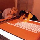
Jules Andrus 和 Walter Bond 应用光刻蚀法技术从印刷工艺到能够在晶圆上精确刻蚀扩散成一个窗口 在 1955 年 Jules Andrus 和 Walter L. Bond 在贝尔实验室 开始把现有的光刻技术(也被称为照相制版)技术开发制造模式应用于印刷电路板使生产更精确, 在硅晶片用到了 更复杂的基于 Frosch 和 Derick’s 二氧化硅层的 设计 。 ( 1955 里程碑)在应用光敏涂料或 “ 抵抗 ” 的层和揭露所需的图案涂层,通过光掩膜,精确的窗口地区被定义在层和化学蚀刻,抵制开幕暴露被冲走。杂质通过这些口扩散到基本硅建立区的 n 型和 p 型硅半导体器件。 1957 年, 在早期的尝试以小型电子电路,杰伊莱斯罗普杰姆斯所有的美国陆军军械引信实验室钻石在马里兰州专利光刻技术用于沉积薄膜的金属条,约 200 微米宽连接离散晶体管的一个陶瓷基板。他们还使用这些技术的蚀刻孔二氧化硅制造二极管阵列。 1959 年, Lathrop 加入了德州仪器,致力于集成电路研究, Nall 去了飞兆半导体。 随后该创举, 1958 年在飞兆半导体公司, Jay Last 和 Robert Noyce 创造了第一个单反相机,应用光刻技术使在一个硅晶片上有很多晶体管。在 1961 年 GCA 的一个分公司 David W. Mann 是第一个公司制作商业步骤,使用重复掩膜来减少设备。 随着特征尺寸低于 0.1 微米变得司空见惯的半导体制造的今天,光刻是一个必不可少的步骤。 译者:哈尔滨工业大学(威海)电子封装-090840119-乔云飞 校对:哈尔滨工业大学(威海)电子封装技术 090840218 赵家玮 原文: http://www.computerhistory.org/semiconductor/timeline/1955-Photolithography.html 版权 copyright by www.computerhistory.org Hand cutting an IC design onto rubylith material for creating the pattern to be optically shrunk onto a photographic mask - early 1970s( 70年代早期, 手工切割 集成电路 设计 ) A completed rubylith layer ready for photographic reduction - circa 1965(一个 完好的 红膜 层显影) Figure from 1957 Lathrop, et al. semiconductor fabrication patent( 图 1957 莱思罗普, 半导体制造 专利 ) Burt Wheeler developed the Mann photorepeater for making masks( 伯特研究出摄影复印机 ) Jules Andrus and Walter Bond adapt photoengraving techniques from printing technology to enable precise etching of diffusion "windows" in silicon wafers. In 1955 Jules Andrus and Walter L. Bond at Bell Labs began adapting existing photolithographic (also called photoengraving) techniques developed for making patterns on printed circuit boards to produce much finer, more intricate designs on silicon in wafers using Frosch and Derick’s silicon-dioxide layer. ( 1955 Milestone ) After applying a photosensitive coating or "resist" on the layer and exposing the desired pattern on this coating through an optical mask, precise window areas were defined in the layer and opened by chemical etching where unexposed resist had been washed away. Impurities were diffused through these openings into the underlying silicon to establish the zones of n -type and p -type silicon needed in semiconductor devices. In an early attempt to miniaturize electronic circuits in 1957, Jay Lathrop and James Nall of the U.S. Army’s Diamond Ordnance Fuse Laboratories in Maryland patented photolithographic techniques used to deposit thin-film metal strips about 200 micrometers wide to connect discrete transistors on a ceramic substrate. They also used these techniques to etch holes in silicon dioxide to fabricate diode arrays. In 1959 Lathrop joined Texas Instruments, working for Jack Kilby, and Nall went to Fairchild Semiconductor. Following up on this pioneering work, Jay Last and Robert Noyce built one of the first "step-and-repeat" cameras at Fairchild in 1958 to make many silicon identical transistors on a single wafer using photolithography. In 1961 the David W. Mann division of GCA Corporation was the first firm to make commercial step and repeat mask reduction devices (photo-repeaters). Photolithography remains an essential step in semiconductor manufacturing today, with feature sizes below 0.1 micrometer becoming commonplace.
1958年 - 所有半导体固态电路得以证明 杰克.基尔比用半导体材料制造了一个兼有主动与被动部分的微型电路。 随着计算机系统变得更加复杂,工程师们也在寻求更加简单的方法去连接他们所使用的数以万计的晶体管。政府机构资助微型模块和多芯片混合电路工程来解决这个问题。 1952 年,英国电信研究机构的 GWA Dummer 提出“随着晶体管的问世和半导体领域的广泛研究,现在看来可以设想出一种没有连接线的电子设备,并使之封闭于一个固体块中。” 从 50 年代中期到后期,一系列的项目成功地将多个组件集成于一个芯片上。在美国无线电公司, Harwick Johnson 取得了一个无线电振荡器专利, Torkel Wallmark 和 Sanford Marcus 分别创立了移位寄存器和逻辑门。 阿瑟 · 德阿萨罗和伊恩 · 罗斯贝尔实验室制作出了电话应用方面的四阶段计数器。 IBM 公司的乔 · 罗格和里克 · 迪尔制作出了一台使用双基极二极管结构的电脑。日本通产省的 Yasuro Tarui 和德州仪器的 Richard Stewart 提交了多个设备专利。 麻省理工学院的 Dudley Buck 研发了一种超导集成元件制成的低温管。尽管这些成就取得了不同程度的功能,但是没有一个可以解决通用性的系统集成带来的挑战。 1958 年 9 月 12 日,来自德州仪器的 Jack Kilby 在锗基片上用 PNP 型晶体管自己刻蚀制作了一个含有晶体管、电阻、电容等原件的电路。通过使用精致的金制“神奇导线”,他将各自分立的原件连接到了一个振荡电路。一个星期之后,他制作出了放大器。德州仪器在 1959 年 3 月宣布了 Kilby 的“固体电路”概念,并在 1960 年 3 月推出其首个商业设备, 502 型号的二进制触发器,每个售价为 450 美元。但是金线互联并不是一个实用的生产技术。 1961 年 10 月,德州仪器推出的 51 系列直接藕合晶体管逻辑 “ 完全集成电路 ” 系统,使用敷金属平面技术( 1959 年里程碑) 。 图一: Jack Kilby with his lab notebook open at his first solid circuit drawing 杰克 · 基尔比与他的实验室笔记本,展示了他的第一固体电路图纸 Courtesy of: Texas Instruments, Inc 图二: Kilby’s original germanium multi-chip "solid-circuit" oscillator Kilby 的原锗多芯片 “ 固体电路 ” 振荡器 Courtesy of: Texas Instruments, Inc 图三: Connection diagram and open package photograph of the Type 502 flip-flop with "flying-wire" internal connections 连接图和 502 型 “ 飞线 ” 的封装内部连接触发器 Courtesy of: Texas Instruments, Inc 图四: G.W.A. Dummer predicted "solid block" circuits in 1952 G.W.A. dummer 1952 年预测 “ 固体块 ” 电路 Credit: Robert Cathles, under GNU Free Documentation License 译者:哈尔滨工业大学(威海)电子封装 090840123-薛彦峰 校对:哈尔滨工业大学(威海)电子封装 090840125-赵宏博 原文: http://www.computerhistory.org/semiconductor/timeline/1958-Miniaturized.html 版权 copyright by www.computerhistory.org 原文: 1958 - All semiconductor "Solid Circuit" is demonstrated Jack Kilby produces a microcircuit with both active and passive components fabricated from semiconductor material. As computer systems grew more complex, engineers sought simpler ways to interconnect the thousands of transistors they employed. Government agencies funded micro-module and multi-chip hybrid circuit projects in search of a solution to this problem. In 1952, G. W. A. Dummer of England's Telecommunications Research Establishment proposed "With the advent of the transistor and the work in semiconductors generally, it seems now possible to envisage electronic equipment in a solid block with no connecting wires." From the mid to late 1950s several projects succeeded in integrating multiple components on a chip. At RCA Harwick Johnson patented an oscillator and Torkel Wallmark and Sanford Marcus built shift registers and logic gates. Arthur D'Asaro and Ian Ross of Bell Labs fabricated a four-stage counter for telephone applications. Joe Logue and Rick Dill of IBM built a counter using a double-base diode structure. Yasuro Tarui of Japan's MITI and Richard Stewart of TI filed multiple device patents. Dudley Buck of MIT developed the cryotron, an integrated superconducting element. While achieving various degrees of functionality, none of these ideas yielded a solution to the challenge of general-purpose system integration. On September 12, 1958, Jack Kilby of Texas Instruments built a circuit using germanium mesa p-n-p transistor slices he had etched to form transistor, capacitor, and resistor elements. Using fine gold "flying-wires" he connected the separate elements into an oscillator circuit. One week later he demonstrated an amplifier. T.I. announced Kilby's "solid circuit" concept in March 1959 and introduced its first commercial device in March 1960, the Type 502 Binary Flip-Flop priced at $450 each. However the flying-wire interconnections were not a practical production technique. In October 1961, T.I. introduced the Series 51 DCTL "fully-integrated circuit" family using deposited-metal planar technology ( 1959 Milestone ).
1959 年 “ 平面 ” 制造工艺的发明 Jean Hoerni 发展平面工艺解决了晶体管可靠性问题 , 从而使半导体制造革命化。 与台面晶体管( 1958 里程碑)的可靠性问题寻求解决方案, Fairchild 的物理学家 Jean Hoerni 回忆起他曾在 1957 年 12 月记录的想法 — 一个新的进程,在离开氧化层的硅片上,以保护敏感的 PN 下面的路口。由于专注于首批设备的投入生产,在那时该公司没有追求这种做法。 由于担心可能的污染物,传统的智慧,也需要去除氧化物掩蔽完成后这一层,从而暴露了路口。 Hoerni 观看氧化物,而不是作为一种可能的解决方案 - 他的“平面”的方法,成品设备的地势平坦而命名,会保护这些路口。在 1959 年 1 月编写了专利披露后,那年三月,他证明了工作平面晶体管的存在。就像霍尔尼曾预言过的,确实发现氧化层保护的路口。 平面器件也被证明有更好的电气特性 - 尤其是远低漏电流,这是计算机逻辑设计中的关键。他们允许从一个晶圆( 1960 里程碑)侧面制造集成电路的所有组件。 1960年4月,仙童公司推出了商业性的2N1613平面晶体管,并注册了该工艺在工艺中的所有权。今天的 10 亿个晶体管的集成电路全部依靠的是 Hoerni 的突破性理念。一位历史学家称它是“在半导体产业史上最重要的创新。” 虽然平面技术使硅晶体管以满足航空航天工业的严格要求,但是半导体厂商在遇到的每一个重大的技术进步的同时也会遇到新的麻烦。在 20 世纪 60 年代的重大问题,包括金丝上的“紫色的瘟疫”,铝与电的连线,和 MOS 晶体管的稳定。 1964 年(里程碑) 图一: 1 Jean Hoerni with transistor geometry in the background Jean Hoerni 在晶体管几何背景下的的照片 图二: Photomicrograph of a Model 2N1613 planar transistor 2N1613 平面晶体管模型的照片 图三: Figure from Hoerni’s patent on the planar manufacturing process Hoerni 的从图上显示的平面制造工艺过程的照片 图四: Cutaway view of an early Fairchild planar transistor 早期 Fairchild 平面晶体管的剖视图 译者:哈尔滨工业大学(威海)电子封装 090840124-于凯先 校对: 原文: http://www.computerhistory.org/semiconductor/timeline/1959-invention-of-the-planar-manufacturing-process-24.html 版权 copyright by www.computerhistory.org 原文: 1959 - Invention of the "Planar" Manufacturing Process Jean Hoerni develops the planar process to solve reliability problems of the mesa transistor, thereby revolutionizing semiconductor manufacturing. Seeking a solution to reliability issues with the mesa transistor ( 1958 Milestone ), Fairchild physicist Jean Hoerni recalled an idea he had recorded in December 1957 - a new process in which the oxide layer is left in place on the silicon wafer to protect the sensitive p-n junctions underneath. Focused on getting its first devices into production, the company did not pursue the approach at that time. Due to concerns about possible contaminants, conventional wisdom required removing this layer after completion of oxide masking, thus exposing the junctions. Hoerni viewed the oxide instead as a possible solution - his "planar" approach, named after the flat topography of the finished device, would protect these junctions. After writing a patent disclosure in January 1959, he demonstrated a working planar transistor that March. The oxide layer was indeed found to protect the junctions, as Hoerni had predicted. Planar devices also proved to have better electrical characteristics - particularly far lower leakage currents, which is critical in computer logic design. And they permitted fabrication of all the components of an integrated circuit from one side of a wafer ( 1960 Milestone ). Fairchild introduced the 2N1613 planar transistor commercially in April 1960 and licensed rights to the process across the industry. The billion-transistor integrated circuits of today rely on Hoerni’s breakthrough idea. One historian has called it "the most important innovation in the history of the semiconductor industry." While planar technology enabled silicon transistors to meet the stringent demands of the aerospace industry, semiconductor vendors continued to encounter new failure mechanisms with every major technology advance. Significant issues in the 1960s included “purple plague” on gold bonding wires, electromigration of aluminum interconnect lines, and MOS transistor stability. ( 1964 Milestone )
1960-第一个平面集成电路的制作 Jay Last引领了基于Hoerni的平面法和Noyce的整体方法的第一个商用IC的发展。 1959年8月Fairchild半导体研发主任Robert Noyce让共同创立者Jay Last开始开发一个基于Hoerni的平面法(1959里程碑)和Noyce的专利(1959里程碑)的平面集成电路。在Wescon用分立晶体管建立了一个多芯片触发器来诠释概念之后,Last组成了一个包括Sam Fok, Isy Haas, Lionel Kattner, 和 James Nall的团队。根据应用部门的Don Farina, Robert Norman提供的特性化数据,用一个改良的直接耦合晶体管逻辑(DCTL)电路设计了一个带有4晶体管和5个电阻器的兼有早期平面处理能力集成电路。 在一个芯片上集成多重相连的装置造成了许多新的工程挑战。1960年5月26日生产的第一个工作的单块集成电路设备使用了物理隔离来实现组件之间的电隔离。硅晶圆的背面刻蚀了深凹槽并且充满了不导电的环氧树脂。由Haas and Kattner研发的用硼扩散技术来实现p-n节电子隔离成为了首选的生产方法,并在1960年9月27日投入了集成电路的生产。 1960年Fairchild在工程会议提出了先进的信息并提供了面向的客户原型样品。在名为Logic (Micrologic)的贸易下,”F” 类型触发器功能在1961年通过一个在纽约的新闻发布会上展示广告和《生活》杂志上的一张照片向社会公告。五个包括" G "类型门功能(1962里程碑),半加法器和一个半移位寄存器的外加的电路在10月被应用。 Jay Last with Gordon Moore in background Jay Last和Gordon Moore在背景下 Credit: Fairchild Camera Instrument Corporation Physically-isolated Micrologic flip-flop compared to a dime from LIFE magazine March 10, 1961 物理隔离的微程序控制逻辑触发器与硬币相比,摘自1961年3月10日的生活杂志 Credit: Fritz Goro, Time Life Pictures Junction-isolated version of the type "F" flip-flop. The die were etched to fit into a round TO-18 transistor package 节孤立版本的“F”类型触发器。晶片被蚀刻来适应一个圆TO-18晶体管封装。 Credit: Fairchild Camera Instrument Corporation Presentation block with a Micrologic wafer and IC in the TO-18 package 一个微程序控制逻辑晶圆和集成电路在圆TO-18晶体管封装中的展示块 CHM collection: Gift of Bob and Marcella Major 译者:哈尔滨工业大学(威海)电子封装 090840126-种兆永 校对:哈尔滨工业大学(威海)电子封装 090840124-于凯先 原文 http://www.computerhistory.org/semiconductor/timeline/1960-FirstIC.html 版权 copyright by www.computerhistory.org ———————————————————————————————————— 1960 - First Planar Integrated Circuit is Fabricate Jay Last leads development of the first commercial IC based on Hoerni’s planar process and Noyce’s monolithic approach. In August 1959 Fairchild Semiconductor Director of RD, Robert Noyce asked co-founder Jay Last to begin development of an integrated circuit based on Hoerni’s planar process ( 1959 Milestone ) and Noyce’s patent. ( 1959 Milestone ) After building a multi-chip flip-flop with discrete transistors to demonstrate the concept at Wescon, Last assembled a team including Sam Fok, Isy Haas, Lionel Kattner, and James Nall. Based on characterization data prepared by Don Farina, Robert Norman of the applications department designed a flip-flop with four-transistors and five resistors using a modified Direct Coupled Transistor Logic (DCTL) circuit as most compatible with early planar processing capabilities. Integrating multiple interconnected devices on one chip posed many new engineering challenges. The first working monolithic devices produced on May 26 1960 used physical isolation to achieve electrical separation between components. Deep channels were etched from the rear of the silicon wafer and filled with non-conducting epoxy. The preferred production method, p-n junction electrical isolation using a boron diffusion technique developed by Haas and Kattner, yielded working circuits on September 27, 1960. Fairchild presented advanced information at engineering conferences and provided prototype samples to customers in 1960. Under the trade name Logic (Micrologic), the type "F" flip-flop function was announced to the public in March 1961 via a press conference at the IRE Show in New York and a photograph in LIFE magazine. Five additional circuits, including the type "G" gate function ( 1962 Milestone ), a half adder, and a half shift register, were introduced in October.
图1 Dawon Kahang的金属氧化物半导体(mos)晶体管的图形 M. M. (John) Atalla and Dawon Kahn g 在 1995 年于贝尔实验室成功制造了第一个绝缘栅极场效应晶体管,一直被 Lilienfeld, Heil, Shockley 等人长期期望的通过注入到半导体材料来克服表面态从而封锁电场。通过研究二氧化硅热生长层,他们发现这些 ** 会在一个由金属(金属极),氧化物(氧绝缘层),硅(硅半导体)组成的三明治(也就是 金属氧化物半导体场效应晶体管,通常被成为金属氧化物半导体 )的硅及其氧化物之间有一个明显的减小。因为他们的装置缓慢而起在电话系统中没有很急切的需求,所以它没有进一步的发展。在一个 1961 年的备忘中, Kahng 却指出了它在易于制造和在集成电路方面应用的可能性的潜力,飞兆半导体和美国无线电公司的研究人员认识到了这些优势。在 1960 年 Karl Zaininger 和 Charles Meuller 在美国无线电公司制造了一个 金属氧化物半导体晶体管,飞兆半导体的 C.T. Sah 制造了一个可控金属氧化物半导体四极管。 Fred Heiman and Steven Hofstein 随后在美国无线电公司于 1962 年研制出了 实验用 16 个晶体管的集成装置。 图2仙童半导体的FI 100 的p沟道金属氧化物半导体开关晶体管 金属氧化物半导体晶体管的导电区域要么是 p 型 ( 称其 p 沟道 设备 ) 或 n 型 (n- 沟道设备 ) 材料,后者要比 p 沟道的更快,同时也更难制作。 金属氧化物半导体器件 在 1964 年冲击了商业市场。通用微电子公司和飞兆半导体公司将 p 型装置用于逻辑开关。美国无线电公司引进了一种 n 沟道的晶体管用于放大信号。由于它比双极性器件有更小的尺寸和功率消耗,如今超过百分之 99 的微型芯片都用金属氧化物半导体器件来制作。取得这样的普遍应用耗费了十年努力。 图3 RCA16金属半导体晶体管的电路放大图像 图4 1962年在RCA的 MOS IC开发者 Steven Hofstein 译者:哈尔滨工业大学(威海)电子封装 090840127-周超 校对:哈尔滨工业大学(威海)电子封装 090840128- 徐涛 原文 http://www.computerhistory.org/semiconductor/timeline/1978-PAL.html 版权 copyright by www.computerhistory.org ———————————————————————————————— 1960 - Metal Oxide Semiconductor (MOS) Transistor Demonstrated John Atalla and Dawon Kahng fabricate working transistors and demonstrate the first successful MOS field-effect amplifier. In 1959 M. M. (John) Atalla and Dawon Kahng at Bell Labs achieved the first successful insulated-gate field-effect transistor (FET), which had been long anticipated by Lilienfeld, Heil, Shockley and others ( 1926 Milestone ) by overcoming the surface states that blocked electric fields from penetrating into the semiconductor material. Investigating thermally grown silicon-dioxide layers, they found these states could be markedly reduced at the interface between the silicon and its oxide in a sandwich comprising layers of metal (M - gate), oxide (O - insulation), and silicon (S – semiconductor) - thus the name MOSFET, popularly known as MOS. As their device was slow and addressed no pressing needs of the telephone system, it was not pursued further. In a 1961 memo, however, Kahng pointed out its potential ease of fabrication and the possibility of application in integrated circuits. But researchers at Fairchild and RCA did recognize these advantages. In 1960 Karl Zaininger and Charles Meuller fabricated an MOS transistor at RCA and C.T. Sah of Fairchild built an MOS-controlled tetrode. Fred Heiman and Steven Hofstein followed in 1962 with an experimental 16-transistor integrated device at RCA. The MOS transistor conducting region is either p -type (making it a p -channel device) or n -type ( n -channel device) material. The latter are faster than p -channel but are more difficult to make. MOS devices hit the commercial market in 1964. General Microelectronics (GME 1004) and Fairchild (FI 100) offered p -channel devices for logic and switching applications; RCA introduced an n -channel transistor (3N98) for amplifying signals. Because of their smaller size and lower power consumption than bipolar devices, over 99 percent of microchips produced today use MOS transistors. Achieving such ubiquity took decades of effort. ( 1964 Milestone )
1960年外延沉积过程中提高晶体管的性能 薄膜晶体生长过程的发展,导致具有高转换速度的晶体管。 1951年,戈登舠尔和霍华德克里斯滕森在贝尔实验室开发的一个现在被称为外延沉积过程,此过程成长在基板上,继续底层基板上成长一层薄的材料晶体结构。 sheftal',Kokorish,和Krasilov在苏联1957年描述过硅和锗类似的工作过程。 在伊恩圠斯的敦促下,1960年由亨利瘠鶖尔领导的贝尔实验室团队用化学气相沉积增加基层和晶体管集电极之间的薄硅外延层。这种方法不仅提高了晶体管的击穿电压同时显著提高了开关速度(1961年的里程碑)这两个重要的电路设计特点。额外的工艺步骤添加的制造成本比被设备改善的性能还要多。这项技术很快的传到了西方电气公司,并在通过贝尔系统转换的电子电话硅晶体管的制造业中使用。 陶依尔的一个外延晶体管的介绍在1960年6月的固态设备研究会议引起了广泛的关注。 Fairchild公司用外延工艺制造的2N914,在1961年3月推出其最成功之一的晶体管,并迅速被Rheem, Sylvania和Texas仪器公司效仿。 摩托罗拉将此工艺应用在大规模生产汽车交流发电机设备过程中, 硅外延工艺在早期双极集成电路制造业产量的重要影响,使个别电路元件电气隔离的完成更加容易。后来广泛应用在MOS产品制造生产中。外延生长技术也常用在形成超薄层的复合半导体制造中。 图一 伊恩罗斯作为贝尔实验室的董事长的素描像 Pencil sketch of Ian Ross as president of Bell Labs 2006-2007 Alcatel-Lucent. All rights reserved 图2 单一外延工艺反应装置图 Diagram of a simple epitaxial reactor 2006-2007 Alcatel-Lucent. All rights reserved 图3 在运行当中的外延反应装置研究模型图 A research-scale epitaxial reactor in operation Credit: University of South Carolina 图4 外延晶体管在贝尔数字切换系统的应用图 Epitaxial transistors were used in the Bell Number One ESS switch Credit: ATT Corporate History 译者:哈尔滨工业大学(威海)电子封装 090840128-徐涛 校对:哈尔滨工业大学(威海)电子封装 090840127-周超 原文 http://www.computerhistory.org/semiconductor/timeline/1960-Epitaxial.html 版权 copyright by www.computerhistory.org 1960 - Epitaxial Deposition Process Enhances Transistor Performance Development of thin-film crystal-growth process leads to transistors with high switching speeds. In 1951 Gordon Teal and Howard Christensen at Bell Labs developed a process, now called epitaxial deposition, to grow a thin layer of material on a substrate that continues the underlying crystalline structure. Sheftal’, Kokorish, and Krasilov described similar work on germanium and silicon in the U.S.S.R. in 1957. At the urging of Ian Ross, a Bell Labs team led by Henry Theurer used chemical-vapor deposition to add a thin epitaxial layer of silicon between the base and collector of a transistor in 1960. This approach raised the transistor’s breakdown voltage while dramatically increasing its switching speed, (1961 Milestone) two important circuit-design characteristics. The added manufacturing cost of the extra process step was more than offset by improvements in device performance. The technology was quickly transferred to Western Electric and used in manufacturing silicon transistors for electronic telephone switching in the Bell System. Theurer gave a presentation on epitaxial transistors at the June 1960 Solid-State Device Research Conference that aroused widespread interest. Fairchild used epitaxy to fabricate the 2N914, one of its most successful transistors introduced in March 1961 and quickly emulated by Rheem, Sylvania, and Texas Instruments. Motorola applied the process to mass produce devices for automotive alternators. Epitaxial silicon also had an important impact on the manufacturing yield of early bipolar integrated circuits by allowing electrical isolation of the individual circuit components to be accomplished much more easily. It later found widespread application in the manufacture of MOS products. Epitaxial growth techniques are also used to form the ultra-thin layers common in compound-semiconductor manufacturing.
1961- 硅晶体管超过锗晶体管的速度 计算机工程师 西摩 · 克雷基金发展第一个硅装置来满足世界上最快机器的性能要求。 在通用自动电子计算机方面,计算机工程师西摩 · 克雷曾经致力于通用晶体管公司的锗晶体管。在和 威廉 · 诺里斯一成立数据控制公司,克雷就让通用晶体管公司为 CDDC 1604 计算机生产出了快速切换的锗设备,这个计算机在 1960 年成为了第一个商业成功的大型科学计算晶体管机器。 为了创造世界上最快的超级计算机,克雷要求一个在成百上千设备近距离工作产生的高温环境中运行且能在 3 纳秒之内切换的晶体管。 克雷授予飞兆半导体公司 500 , 000 美元的开发合同要为 CDC 6600 制造一个新的晶体管。 吉恩 · 赫尔尼达到了技术要求,结合 “ 掺金 ”—— 除了黄金杂质 - 连同新的外延沉积过程。该 2n709 ( ft-1310npn 型装置)在 1961 年 7 月作为第一类超越锗速度的硅晶体管被介绍推出。 每一个 CDC 6600 用 600 , 000 个晶体管封装在一个独特的 cordwood-style 模块配置中来减少连接电线的长度。在 1964 年飞兆半导体因为超过一千万的设备被成为“半导体产业历史上最大的单一指令之一”。科学数据系统是另一个在西格玛系列电脑逻辑应用中高速硅半导体的早期采纳者。 Jean Hoerni working in the lab 图片 1 :吉恩 · 赫尔尼正在实验室工作。 。 2N709 die - epitaxial gold-doped switching transistor 图片 2 : 2N709 晶圆外延开 掺金开关晶体管。 CDC 6600 "cordwood-module" transistor-based logic units 图片 3 : CDC 6600”cordwood 模块 ” 电晶体逻辑组合。 Open logic and memory "leaves" of a CDC 6600 图片 4 : CDC 6600 的开放式逻辑与记忆的“叶子”。 版权 copyright by www.nobeprize.org 译者:哈尔滨工业大学(威海)电子封装 090840129-祝乐 校对:哈尔滨工业大学(威海)电子封装 090840112-李迪 1961 - Silicon Transistor Exceeds Germanium Speed Computer architect Seymour Cray funds development of the first silicon device to meet the performance demands of the world’s fastest machine. Computer architect Seymour Cray had worked with General Transistor Corporation’s germanium transistors at Univac. On founding Control Data Corporation in 1957 with William Norris, Cray asked General Transistor to develop a fast switching germanium device for the CDC 1604 that in 1960 became the first commercially successful large-scale transistor machine for scientific computing. With the goal of building the world’s fastest supercomputer, Cray required a transistor that switched in less than 3 nanoseconds while operating in a high temperature environment created by hundreds of thousands of devices operating in close proximity. Early silicon transistors offered superior operation to germanium at elevated temperature but were too slow for many computer designs. Cray awarded Fairchild Semiconductor a $500,000 development contract to build a new transistor for the CDC 6600. Jean Hoerni met the specification by combining "gold-doping" - the addition of gold impurities - together with the new epitaxial deposition process. ( 1960 Milestone ) The 2N709 (FT-1310) n-p-n device was introduced in July 1961 as the first silicon transistor to exceed germanium speed. Each CDC 6600 used 600,000 transistors packaged in a unique cordwood-style module configuration to minimize connecting wire lengths. In 1964 the company placed "one of the largest single orders in the history of the semiconductor industry" with Fairchild for over 10 million devices. Scientific Data Systems was another early adopter of high-speed silicon transistors for logic applications in the Sigma series computers.
1962年-航天航空系统首先在计算机中应用集成电路 在军事和航空航天系统中,集成电路的尺寸,重量和降低功耗设计相比于分立式晶体管来说更证明了它高成本的合理性。 第一个集成电路仅仅取代了少数元件,速度相对迟缓,但卖价却是它相对应的分立式晶体管价格的好多倍。所以航空航天和军事系统是少数应用这种低功耗和小尺寸的应用程序的系统。 1961 年杰克基尔比的同事哈维克瑞根为美国空军演示“分子的电子化计算机” 来证明 587 个美国德州仪器集成电路在通用设计中可以代替 8500 个晶体管和其它组件来完成同样的功能。 自 1961 年,飞兆半导体微程序控制逻辑装置( 1960 年重要事件)被设计进交流火花塞和马丁马太克 420 计算机中,而不是在美国国家航空和宇宙航行局的阿波罗制导计算机(自动增益控制)中,成为最有意义的早期项目。此装置由麻省理工大学于 1962 年设计,并由雷声公司建成,每个系统大约使用了 4000 个 “G 类型 ” ( 3- 输入或非门)电路。到 1965 年,自动增益控制是集成电路最大的使用者,每个在 20 到 30 美元之间消耗 2000 个单位。 工程师库克设计 51 系列直接耦合晶体管逻辑电路,这是德州仪器的首次平面集成电路系列,以此来满足美国国家航空和宇宙航行局的行星间检测探针( IMP )的光纤层面计算机低功耗的标准。接口信息处理器卫星使用 510 款和 514 款作为二进制计数器,触发器和禁止电路,并于 1963 年携带首个集成电路绕轨道运行。在 1962 年德州仪器赢得一份与北美飞机制造业自动控制部门的合同,来为民兵二的导弹制导系统设计 22 习用电路。可莱维特和西屋电器也为民兵计划制造环路,并且在 1965 年取代了美国国家航空和宇宙航行局的阿波罗电子采购成为唯一一个集成电路的最大消费者。 费兰蒂股份有限公司研发的编码器。属于英国开发的微 NOR ,是欧洲最早的集成电路逻辑系列之一, 1961 年使英国皇家海军系统飞机上的计算机系统小型化。 Philco Ford also produced the Fairchild Type "G" Micrologic gate for the Apollo Guidance Computer Credit: Philco-Ford Microelectronics 飞哥福特还为阿波罗制导计算机生产了“ G ”类型微程序控制逻辑门飞兆半导体 资源出处:飞哥福特微电子科技 Apollo logic module assembled by Raytheon Credit: U. S. National Aeronautics and Space Administration 由雷声公司组装的阿波罗逻辑模块 资源出处:美国国家航空和宇宙航行局 Eldon C. Hall, MIT Instrumentation Laboratory lead hardware designer for the AGC promoted the use of integrated circuits Credit: MIT Archives 埃尔登 C ,麻省理工学院测试试验实验室为自动增益控制促进集成电路的使用主要计算机硬件设计者 资源出处:麻省理工学院档案 TI's "Molecular Electronic Computer" brochure prepared to accompany the demonstration machine on a tour of military contractors Courtesy of: Texas Instruments, Inc. 德州仪器准备在一次军事合约商洽谈中伴随机器示范的“分子化电子计算机”宣传册 提供途径:德州仪器公司 译者:哈尔滨工业大学(威海)电子封装 090840202-顾佳慧 校对:哈尔滨工业大学(威海)电子封装 090840203-李丹 原文 http://www.computerhistory.org/semiconductor/timeline/1962-Apollo.html 版权 copyright by www.computerhistory.org ——————————————————————————————————————————————————————— The size, weight, and reduced power consumption of integrated circuits compared to discrete transistor designs justify their higher cost in military and aerospace systems. The first integr ated circuits were relatively slow, replaced only a handful of components, and sold for many times the price of their discrete transistor counterparts. Aerospace and military systems were among the few applications where the low power consumption and small size outweighed these drawbacks. In 1961 Jack Kilby’s colleague Harvey Cragon built a demonstration "Molecular Electronic Computer" for the US Air Force to show that 587 TI ICs could replace 8,500 transistors and other components that performed the same function in a conventional design. Beginning in 1961, Fairchild Micrologic devices ( 1960 Milestone ) were designed into the AC Spark Plug MAGIC and Martin MARTAC 420computers but NASA's Apollo Guidance Computer (AGC) was the most significant early project. Designed by MIT in 1962 and built byRaytheon, each system used about 4,000 “Type-G” (3-input NOR gate) circuits. Consuming 200,000 units at $20-30 each, the AGC was the largest user of ICs through 1965. Engineer Bob Cook designed Series 51 DCTL, Texas Instruments' first planar IC family, to meet a low-power specification for the Optical Aspect Computer on NASA’s Interplanetary Monitoring Probe (IMP). Using the SN510 and SN514 as binary counters, flip-flops, and inhibiting circuits, the IMP satellite carried the first ICs into orbit in 1963. In 1962 TI won a contract from the Autonetics Division of North American Aviation to design 22 custom circuits for the Minuteman II missile guidance system. Clevite and Westinghouse also developed circuits for the Minuteman project, which by 1965 overtook NASA’s Apollo procurement as the largest single consumer of ICs. Ferranti Semiconductor Ltd. of England developed MicroNOR, one of Europe's first IC logic families, in 1961 to miniaturize on-board computing systems in UK Royal Navy systems.
1963年标准逻辑集成电路家族介绍 二极管 - 晶体管逻辑电路 (DTL) 家族为数字集成电路创造了广大的市场,但是到二十世纪六十年代末期在速度,成本及集成度方面占优势的改进型肖特基晶体管(TTL)成为了最流行的标准逻辑配置。 分离二极管 - 晶体管逻辑电路 (DTL) 的完整版本成为了第一个大量 IC 产品生产线。贝克·奥威尔在 1962 年设计的, se100 系列的 DTL 家族被 Fairchild 的 930 系列创造的一个有竞争力的跳背模式产品以其更小的噪音,更便宜的价格优势所赶超,这种产品一直沿用至今。 Pacific Semiconductor 的 James Buie 在 1961 年申请专利, TTL (晶体管—晶体管逻辑电路)作为以后二十年里最受欢迎的逻辑配置出现。没有注意到 Bule 的成果,但是因为 Ruegg 和 Fairchild 的 Beeson 描绘的“完全晶体管”逻辑电路模型而有了灵感, Thomas Longo 在 1963 年领导设计了第一个 TTL 家族——西尔维尼亚万能高电平逻辑电路( SUHL )。被 SUHL 在凤凰导弹应用的成功所激励, TI 在第二年生产了有竞争力的 TTL 家族的 SN5400 系列 。这个公司在 1966 年发布的 SN7400 系列是为工业顾客设计的低成本的塑料封装,它迅速占领了逻辑领域超过百分之五十的市场。 到 1968 年,平板印刷术很大的增加了整合在芯片上的晶体管的数量,热切地希望在 TTL 产业占一定的份额, Fairchild ( 9300 系列)和 Signetics ( 8200 系列)开拓了 TTL-MSI (中等规模集成—每个芯片上升至 100 个逻辑入口) 结的设计制造,比如计数器,注册转移和算术逻辑部件。一些卖家应用萧特基( 1969 年的里程碑)和互补型金属氧化物半导体( 1963 年的里程碑)技术去建立更大,更快,耗能更低的 TTL 兼容结,它拓宽了有效年限和这种受欢迎的逻辑配置的申请范围。 Introduced 2 years after Signetics SE124 DTL flip-flop, Fairchild's 930 series DTL (right) was smaller and therefore cheaper and faster Credit: Fairchild Camera Instrument Corporation Signetics的SE124DTL触发器引入两年后,Fairchild的930系列DTL更小因此成本更低更快 Dr. Thomas A. Longo developed SUHL TTL at Sylvania in 1963 Credit: Fairchild Camera Instrument Corporation Thomas A. Longo博士于1963年在西尔维尼亚研制了SUHL TTL The indispensable data manual of the 1970s Courtesy of: Texas Instruments, Inc 1970系列必不可少的的数据手册 Am9300 TTL MSI universal shift register. AMD’s first product was an improved version of the Fairchild original CHM Collection. Photo gift of Ed Turney Am9300 TTL MSI 的通用转换缓存器,AMD的第一个产品是一个Fairchild原始版本的改进版 译者:哈尔滨工业大学(威海) 电子封装 090840204-马聪 校对:哈尔滨工业大学(威海)电子封装 090840206-杨英坤 原文: http://www.computerhistory.org/semiconductor/timeline/1963-TTL.html 版权 copyright by www.computerhistory.org 1963 - Standard Logic IC Families introduced Diode Transistor Logic (DTL) families create a high-volume market for digital ICs but speed, cost, and density advantages establish Transistor Transistor Logic (TTL) as the most popular standard logic configuration by the late 1960s. Integrated versions of discrete diode transistor logic (DTL) circuits became the first high-volume IC product lines. Designed by Orville Baker in 1962, the Signetics SE100 Series DTL family was overtaken in 1964 by the better noise immunity and lower cost of Fairchild's 930 Series establishing a competitive industry leap-frog pattern that continues today. Patented by James Buie of Pacific Semiconductor in 1961, TTL (Transistor Transistor Logic) emerged as the most popular logic configuration of the next two decades. Unaware of Buie's work but inspired by an "all transistor" logic circuit described by Ruegg and Beeson of Fairchild, Thomas Longo led the design of the first TTL family, Sylvania Universal High-level Logic (SUHL) in 1963. Encouraged by SUHL's success in winning a high-profile Hughes military design (the Phoenix missile), TI introduced the competing SN5400 Series TTL family the following year. The company announced the SN7400 Series in low cost plastic packages for industrial customers in 1966 and quickly gained a greater than 50% share of the logic market. By 1968 lithography advances significantly increased the number of transistors that could be integrated on a chip. Eager to win a share of the TTL business, Fairchild (9300 Series) and Signetics (8200 Series) pioneered the design of TTL-MSI (Medium Scale Integration - up to 100 logic gates per chip) functions such as counters, shift registers, and arithmetic logic units. Many vendors applied Schottky ( 1969 Milestone ) and CMOS ( 1963 Milestone ) technology to build larger, faster, and lower power TTL-compatible functions that extended the useful life and range of applications of this popular logic configuration.
半导体里程 _ 博物馆 _ 第一个商业MOS集成电路的介绍 Andy Grove, Bruce Deal, and Ed Snow discuss MOS technology at the Fairchild Palo Alto R D laboratory in 1966 Credit: Fairchild Camera Instrument Corporation 图一 安迪 · 格鲁夫 , 布鲁斯 · 帝尔 , 艾德 · 雪飞在帕洛阿尔托的飞兆半导体研发实验室探讨 MOS 技术于 1966 年 一般微电子使用一种金属氧化物半导体 (MOS) 处理来在芯片上装比双极集成电路更多的晶体管,并使用这项技术建立了第一个计算器芯片组。 由于复杂的制造和可靠性问题,所以实现 MOS 关于比双级( 1960 里程碑)高密度和低成本的承诺比预期的更困难。在研讨会上的发言者把在电子学方面的失败的物理现象与盲人摸象的故事做比较 -— 这主要取决于你检查哪一部分。 1961 年弗雷德里克· 海曼 和史蒂文·奥弗斯坦在美国无线电公司做了个关于 16 晶体管集成电路的实验并且后来在了解表面氧化物质量方面做出了重要贡献。在 1963 年和 1966 年之间,布鲁斯·帝尔,安德鲁·格鲁夫和艾德·雪尔在仙童 半导体公司 鉴定了纳污染问题并且出版了很多关于氧化物的电性性质的论文这些为格鲁夫的经典教材《物理和半导体设备技术》提供了资料。世界各地的合作与竞争,包括来自 NEC · IBM ·飞利浦的研究者在最后的十年中解决了基本的产量和可靠性问题使得 MOS 作为主导的 IC 技术出现。 R. P. Donovan’s illustration of the spectrum of MOS instability explanations presented at a 1966 symposium Courtesy of: Bruce Deal and Harry Sello 图二 R.P 多诺万的关于 MOS 不稳定性的图解在 1966 年的一个研讨会上呈现 The first commercial MOS IC, GMe's 20-bit shift register used 120 p-channel transistors in 1964 CHM Collection. Photo gift of Don Farin 图三 第一个用了 120 个通道的 晶体管的商用 MOS IC 、 GMe 的 20-bit 移位寄存器在 1964 年 1964 年当罗伯特·诺曼使用一个二阶段时钟计划来设计一个用 120p 通道晶体管的 20 位移位寄存器时,普通的微电子推出了第一个商业 MOS 集成电路。 1965 年, GMe 作为第一个基于 MOS 的电子计算操纵者为 维克特康普托计算机 设计了 23 位自定义集成电路。 飞哥福特 收购了该公司并且将业务转移到费城大多数员工转移到其他公司后,在 航空英里指示器 及通用仪器方面继续蓬勃发展计算机芯片市场。 The prototype Victor Comptometer EC-3900 calculator and board with 23 custom MOS chips and six 100-bit shift registers for serial memory CHM Collection. Gift of Don Farina 图四康普托计算机原型 EC- 3900 计算器和在 23 个自定义 MOS 芯片和六个 100 位移位寄存器和串行存储器 到 1969 年罗克韦尔微电子学为夏普的第一台便捷携带式机 microCompet QT-8D 已经将电子芯片数降到四台设备,并且继续前进成为上世纪 70 年代早期的计算机芯片最大供应商。 1971 年 泰克 及 美国德州仪器公司(1974 里程碑 ) 介绍了单片机 ( 除了外部显示器 ) 驱动程序解决方案 。 译者:哈尔滨工业大学(威海)电子封装 090840206- 杨英坤 校对:哈尔滨工业大学(威海)电子封装 090840204 马聪 原文 http://www.computerhistory.org/semiconductor/timeline/1964-Commecial.html 版权 copyright by www.computerhistory.org ——————————————————————— 1964 - First Commercial MOS IC Introduced General Microelectronics uses a Metal-Oxide-Semiconductor (MOS) process to pack more transistors on a chip than bipolar ICs and builds the first calculator chip set using the technology Achieving the MOS promise of higher density and lower cost than bipolar ( 1960 Milestone ) proved more difficult than anticipated due to complex manufacturing and reliability issues. Speakers at a symposium on the Physics of Failure in Electronics likened competing solutions to the story of the blind man and the elephant – it depends on which part you examine. Frederic Heiman and Steven Hofstein built an experimental 16-transistor IC at RCA in 1961 and later made important contributions to understanding surface oxide quality. Between 1963 and 1966, Bruce Deal, Andrew Grove, and Ed Snow at Fairchild identified the issue of sodium contamination and published many papers on the electrical nature of oxides that informed Grove’s classic textbook Physics and Technology of Semiconductor Devices. Collaboration and competition across the globe, including researchers from NEC, IBM and Philips, resolved the fundamental yield and reliability issues by the end of the decade that allowed MOS to emerge as the dominant IC technology. General Microelectronics introduced the first commercial MOS integrated circuit in 1964 when Robert Norman used a 2-phase clock scheme to design a 20-bit shift register using 120 p-channel transistors. GMe designed 23 custom ICs for the first MOS-based electronic calculator for Victor Comptometer in 1965. After the company was purchased by Philco-Ford and the operation transferred to Philadelphia most employees moved on to other companies, including AMI and General Instrument, where they continued to develop chips for a burgeoning calculator market. By 1969 Rockwell Microelectronics had reduced the chip count to four devices for Sharp's first portable machine, the microCompet QT-8D , and went on to become the largest supplier of calculator chips in the early 1970s. Mostek and TI ( 1974 Milestone ) introduced single-chip (except for external display drivers) solutions in 1971.
1964 年 - 第一个被广泛使用的模拟集成电路出现 大卫塔尔伯特和罗伯特维德勒在飞兆半导体通过建立商业上成功的模拟应用集成电路,开启了一个主要行业部门。 模拟,也称为线性电路,像声音,温度和无线电波那样电路放大和状态信号不断变化的现象。由于处理这些信号需要极高的分辨率,模拟电路要求在设计和制造中有很高的精度。模拟电子管运放的设计是由哥伦比亚大学的研究员露比朱莉的想法一步一步开发的。第一个锗晶体管运放出现在 1958 年,硅晶体管出现在 1960 年。在布尔布朗和菲尔布里克的研究之后不久 nexus 研究室于 1962 年推出第一个预配置的运放模块 。 艾米克,飞兆半导体,莲花,德州仪器和西屋电气公司开发了早期的模拟集成电路。西屋电气公司的林慧聪 1963 年在 Autonetics 民兵 2 导弹的传统运放上使用了片状元件匹配和外侧三极管专利。但是 1964 年由飞兆半导体公司的工艺工程师戴维卡尔伯特和设计师罗伯特韦德的团队发明的 μA702 运放才是第一个被广泛使用的商业产品。 1965 年的继承者 μA709 运放为模拟集成电路建立了巨大的市场。塔尔伯特和韦德在 1965 年末搬到 molectro (后来被国家收购),在那他们通过 lm101 开始建立了一个长久的王朝。然后在 1968 年飞兆半导体的戴维富嘉通过增加一个固有补偿电容第一次升级了 lm101 ,得到 μA741 ,这是有史以来最流行运放。 专业模拟集成电厂商为放大器,比较器,数据转换器,电源管理器件,和汽车,消费,通信应用周边的大量特点发展了广泛的产品目录。模拟器件通常比数字集成电路具有更长的寿命周期。例如有四十年历史的富嘉的 μA741 运放,汉斯 Camenzind Signetics 公司制造的 555 定时器在今天仍被广泛应用。 Robert Widlar inspects the LM10 mask layout circa 1977 Credit: National Semiconductor 罗伯特 · 维德拉 1977 年检查 LM10 版图 An early analog IC, the Fairchild μA700 differential amplifier designed by Bohumil Polata (1963) Credit: Fairchild Camera Instrument Corporation 早期的模拟集成电路,飞兆半导体的 μA700 : Bohumil Polata ( 1963 )设计的差分放大器 Talbert and Widlar's μA709 high-performance operational amplifier (1965) Credit: Fairchild Camera Instrument Corporation 塔尔伯特和维德拉的 μA709 高性能运算放大器( 1965 ) Widlar's LM10 op amp broke new ground for low voltage operation Credit: National Semiconductor 维德拉的 LM10 运算放大器打破了低电压差工作的新局面 译者:哈尔滨工业大学(威海)电子封装 090840207-邹运 校对:哈尔滨工业大学(威海) 原文 http://www.computerhistory.org/semiconductor/timeline/1964-analog.html 版权 copyright by www.computerhistory.org —————————————————————————————————————————————————— 1964 - The First Widely-Used Analog Integrated Circuit is Introduced David Talbert and Robert Widlar at Fairchild kick-start a major industry sector by creating commercially successful ICs for analog applications. Analog, also called linear, circuits amplify and condition signals from continually varying phenomena such as sound, temperature, and radio waves. Because of the nearly infinite resolution required to process these signals, analog circuits demand high precision in design and manufacturing. Analog vacuum tube operational amplifier (op-amp) designs were paced by the concepts developed by Columbia University researcher Loebe Julie. The first germanium transistor op-amp appeared in 1958 with silicon versions in 1960. Nexus Research Labs offered the first pre-configured op-amp modules in 1962 followed shortly by Burr-Brown and Philbrick Researches. Amelco, Fairchild, RCA, TI, and Westinghouse developed early analog ICs. H. C. Lin of Westinghouse employed on-chip component matching and his lateral PNP patent on a custom op amp for the Autonetics Minuteman II missile in 1963. But the Fairchild μA702 op amp, created in 1964 by the team of process engineer Dave Talbert and designer Robert Widlar, was the first widely-used commercial product. Their 1965 successor, the μA709, established a mass market for analog ICs. Talbert and Widlar moved to Molectro (later acquired by National) in late 1965 where they built a linear dynasty beginning with the LM101. Then in 1968 Dave Fullagar of Fairchild one-upped the LM101 by adding an internal compensating capacitor to deliver the μA741, the most popular op-amp of all time. Specialty analog IC manufacturers evolved extensive catalogs of amplifiers, comparators, data converters, power management devices, and numerous specialty circuits for automotive, consumer and communications applications. Analog devices typically have much longer life cyles than digital I/Cs. Examples of 40 year-old designs that remain widely used today include Fullagar's μA741 op-amp and the 555 timer created by Hans Camenzind for Signetics.
1965“摩尔定律”预测 集成电路的发展走向 戈登·摩尔,飞兆半导体公司的研发总监,在一篇内部文献中作了一张图,图中有一条通过五个点的线,代表着1959年至1964年间每片集成电路中一个元器件所需成本的变化情况。摩尔在《集成电子学的未来》这一文献中试图预测未来十年里集成电子学最可能的发展情况。当摩尔以每12个月器件数量翻一番的发展趋势在投影图上进行推断,他发现1975年每个芯片上的器件数目会达到65000个。《让集成电路填满更多元件》作为一篇杂志文章,于1965年4月19日发表在《电子》杂志上。 Gordon Moore at Fairchild R D in 1962 1962年戈登·摩尔在飞兆半导体公司研发中心 Credit: Fairchild Camera Instrument Corporation 在1975年的国际电子器件会议中,摩尔指出光刻方法,晶圆尺寸,工艺技术的发展,以及设备与装置的智能化,尤其是半导体存储器阵列化,能使他发现的规律得意现实。根据更多的近期数据,其中包括更高复杂程度(仅仅比存储器密度低)的微处理器设计,摩尔把未来器件复杂度的增加速率从一年翻一番降为两年翻一番。 Cost vs. time sketch from Moore's 1964 notebook 1964年,戈登·摩尔笔记本中成本与时间关系的草图 Credit: Fairchild Camera Instrument Corporation 这个预测成为一个自我实现的预言,成为半导体工业遵守的一个法则。专家指出年度突破挑战,以确保符合由卡弗·米德命名的“摩尔定律”。1995年,再次回顾产业现状时 (此时英特尔奔腾处理器含有近500万晶体管),摩尔说,“当前的预测是,这样的发展不会马上停止。”一个装置(美国)含有超过十亿个晶体管。 Dr. Moore revisits his projection with additional data gathered through 1975 摩尔博士获取1965年至1975年的新数据之后重新制作的投影图 Courtesy of: Intel Corporation Several of the chips in this photo provided data points for the 1965 article 图中的芯片为1965年发表的那篇文献提供了数据 Credit: Fairchild Camera Instrument Corporation 译者:哈尔滨工业大学(威海)电子封装 090840208-汪洋 校对:哈尔滨工业大学(威海)电子封装 090840209-常青 原文 http://www.computerhistory.org/semiconductor/timeline/1965-Moore.html 版权 copyright by www.computerhistory.org —————————————————————————————————————————————————————— 1965 - "Moore's Law" Predicts the Future of Integrated Circuits Fairchild’s Director of R D predicts the rate of increase of transistor density on an integrated circuit and establishes a yardstick for technology progress. Gordon Moore, Fairchild Semiconductor’s Director of RD, wrote an internal paper in which he drew a line through five points representing the number of components per integrated circuit for minimum cost per component developed between 1959 and 1964. "The Future of Integrated Electronics" attempted to predict "the development of integrated electronics for perhaps the next ten years." Extrapolating the trend to 1975 he projected that the number of components per chip would reach 65,000; a doubling every 12 months. Edited for publication as a magazine article, "Cramming more components onto integrated circuits" was published in Electronics on April 19, 1965. At the 1975 IEEE International Electron Devices Meeting Moore, by now with Intel, noted that advances in photolithography, wafer size, process technology, and "circuit and device cleverness," especially in semiconductor memory arrays, had allowed his projection to be realized. Adding more recent data, that included a higher mix of microprocessor designs that were somewhat less dense than memories, he slowed the future rate of increase in complexity to "a doubling every two years, rather than every year." This prediction became a self-fulfilling prophecy that emerged as one of the driving principles of the semiconductor industry. Technologists were challenged with delivering annual breakthroughs that ensured compliance with "Moore’s Law," as it was dubbed by Carver Mead. On reviewing the status of the industry again in 1995 (at which time an Intel Pentium microprocessor held nearly 5 million transistors) Moore concluded that “The current prediction is that this is not going to stop soon.” Devices exceeding one (U.S.) billion transistors exist today.
1965 主机开始采用集成电路 大型电脑制造商发布了基于定制和特殊用途的集成电路机器。 用于商业和科学计算的大型电子数据处理系统称为“主机”电脑。在十九世纪六十年代,主机供应商通过专有的硬件、操作系统和应用软件在市场上区分他们的系统。他们要求组件能提供不同的特性和比目前可用的通用逻辑系列更快的速度( 1961 年里程碑)。( 1963 年里程碑)由于这些系统提供了大量的商机,飞兆、摩托罗拉、 Signetics 公司、德州仪器及其他手工制作系列的工程师团队都申请定制特殊用途的集成电路。 最早一批设计使用单片集成电路的主机有 1966 年发布的巴勒斯 B2500/3500 、 RCA 光谱 70 系列( 1965 )和科学数据系统西格玛 7 ( 1966 )。巴勒斯的工程师和飞兆的 Robert Seeds 创建了互补晶体管逻辑体系并为惠普的 3000 系列创造了条件。 RCA 创建了电流型逻辑内部电路并与集成电路供应商合作生产它们。 SDS 和 Signetics 及另外几家公司合作完成一个六个设备的系列。 CDC 、通用电气、霍尼韦尔、 IBM 、 NCR 、 SDS 和 UNIVAC 等公司都创建了定制电路系列。 1962 年 1 月, Narud 领头创建了摩托罗拉的 MECL ( Motorola Emitter Coupled Logic 摩托罗拉发射极耦合逻辑)系列,一种单片实施了 IBM 公司基于晶体管的高速逻辑电路。虽然作为标准产品,昂贵的多层印制电路板和系统对冷却的要求限制了数据控制公司、 Cray 公司、通用电气、日立、 ICL 及其他公司对大量电子元件在科学计算机上的使用要求。 1976 年,每个克雷一号机器消耗 25 万对飞兆公司提供的 F100K 元件开关包,每个开关的转换时间都在 1ns 以内。 Describes how to specify a custom IC from Fairchild 图一 介绍如何从飞兆半导体公司定制指定的集成电路 Credit: Fairchild Camera Instrument Corporation A custom TTL gate design from 1964 图二 1964年设计的自定义TTL门电路 Credit: Fairchild Camera Instrument Corporation Burroughs B25/3500 Series used CTL ICs from Fairchild ITT 图三 飞兆半导体和ITT生产的巴勒斯B25/3500系列CTL集成电路 Credit: Burroughs Corporation RCA Custom CML circuits for the Spectra 70 computer 图四 RCA公司为光谱70计算机制造的CML集成电路 Credit: RCA Incorporated 译者:哈尔滨工业大学(威海)电子封装 090840209-常青 校对:哈尔滨工业大学(威海)电子封装 090840208-汪洋 原文 http://www.computerhistory.org/semiconductor/timeline/1965-Custom.html 版权 copyright by www.computerhistory.org ———————————————————————————————— 1965 - Mainframe Computers Employ ICs Large computer manufacturers announce machines based on custom and special purpose integrated circuits. Large electronic data processing systems for business and scientific applications are called "mainframe" computers. In the 1960s mainframe vendors distinguished their systems in the marketplace through proprietary hardware, operating systems, and applications software. They demanded components offering unique features and significantly faster speed (1961 Milestone) than the currently available general-purpose logic families. (1963 Milestone) As these systems offered high-volume production business opportunities, teams of engineers at Fairchild, Motorola, Signetics, TI, and others handcrafted families of custom and special purpose ICs for these applications. Some of the earliest mainframe designs to use monolithic ICs were the Burroughs B2500/3500 announced in 1966, RCA Spectra 70 series (1965), and Scientific Data Systems Sigma 7 (1966). Burroughs engineers cooperated with Robert Seeds at Fairchild to develop a Complementary Transistor Logic (CTL) family that also powered Hewlett-Packard’s 3000 Series. RCA developed Current Mode Logic (CML) circuits internally and worked with IC vendors to manufacture them. SDS worked with Signetics and others on a family of six devices. CDC, General Electric, Honeywell, IBM, NCR, SDS,and Univac also developed custom circuit families. In 1962 Jan Narud led the development of Motorola's MECL (Motorola Emitter Coupled Logic) family, a monolithic implementation of IBM's transistor-based very high speed logic circuits. Although offered as standard products, expensive multi-layer p.c. boards and system cooling requirements limited ECL usage largely to high-performance scientific computer applications at Control Data Corporation , Cray, GE, Hitachi, ICL, and others. In 1976 each Cray 1 machine consumed 250,000 dual F100K ECL gate packages from Fairchild that offered switching times of under 1ns per gate. n
1965- 封装成为系统设计首要问题 摘要: 双列直插的封装格式显著简化 PCB 板布局并降低计算机的组装成本 大多数半导体器件采用陶瓷,金属或塑料等封装形式密封以防止芯片和脆性连接线的损坏。封装工艺尽管具有这样重要的功能,在半导体设计中却是最被疏忽的方面,芯片尺寸过大和功耗过多一直阻碍着封装进程发展。典型的 60 年代的三极管都采用的是带有 3 条外引线的 TO-5 或者 TO-18 金属罐封装。低成本的塑料形式主要用于气密性要求不高的产品,飞兆半导体第一次在最多容纳 10 条外引线的晶体管罐子上安装了微逻辑集成电路。为使航空电子设备上的芯片占有面积最小化,德州仪器的陶荣开发了一种 10 引线 0.25 , ,0125 英寸的扁平封装形式。 · 这些封装迭代大多数源自于现有格式,并不适用于高密度电路板的设计。 1965 年,飞兆半导体的 Don Forbes, Rex Rice, and Bryant ("Buck") Rogers 等人设计了一种 14 引线的,两侧带有 100 密尔的引脚的双列直插式封装形式,这样设计既简化了电路板的布局,又使得器件可自动插入 PCB 板,因此造就了一次计算机制造业的革命。 70 年代前期,低成本,塑料成型版的双列直插封装产量主导了整个产业,并且引脚数一直增加到 64 · 虽然大多数的 DIP 设计采用热压或超声波焊接到纯金或铝导线的芯片,一些厂商尝试用马丁 · 贝尔实验室 Lepselter 发明的微小的焊料凸点互连和改变光束引脚链接的方法,用于高可靠性的应用 前后修边的玻璃密封陶瓷双列直插封装 塑料DIP半剖示意图 摩托罗拉和德州仪器在DEC AXC板上安装的20引脚封装芯片 AMD公司在80年代中期的不同外形的DIP封装 译者:哈尔滨工业大学(威海)电子封装 090840210 高阳 校对:哈尔滨工业大学(威海) 原文 http://www.computerhistory.org/semiconductor/timeline/1978-PAL.html 版权 copyright by www.computerhistory.org 1965 - Package is the First to Accommodate System Design Considerations The Dual In-line Package (DIP) format significantly eases printed circuit board layout and reduces computer assembly cost. · Most semiconductor devices are enclosed in ceramic, metal or plastic packages to prevent damage to the chip and its fragile connecting wires. Despite this important function, packaging was one of the most neglected aspects of semiconductor design. Programs were delayed because the chip was too large or consumed too much power for the designated package. Typical 1960s transistors used TO-5 or TO-18 (Transistor Outline) metal-can packages with three external leads. Lower-cost plastic versions served applications not requiring a hermetic seal . Fairchild mounted its first Micrologic ICs in such transistor cans modified to accommodate up to 10-leads. Yung Tao at Texas Instruments developed a 10-lead, 0.25 by 0.125 inch flat-pack to occupy the smallest possible board area in avionics systems. · Most of these package iterations were derived from existing formats that were not conceived for high-density board designs. In 1965 Don Forbes, Rex Rice, and Bryant ("Buck") Rogers at Fairchild devised a 14-lead ceramic Dual-in-Line Package (DIP) with two rows of pins 100 mils apart that revolutionized computer manufacturing by simplifying layout and allowing automated insertion into printed circuit boards. Low-cost, plastic-molded versions of the DIP outline dominated production volumes by the early 1970s and pin-counts increased up to 64 leads. · While most DIP designs used thermo-compression or ultrasonic bonding to attach fine gold or aluminum wires to the chip, some vendors experimented with tiny solder bump interconnects and variations on a beam-lead approach invented by Martin Lepselter of Bell Labs for high-reliability applications.
1965-4-----半导体只读存储器芯片的出现 半导体只读存储器(光盘)提供高密度和低成本的单位比特 作为在制造过程中被写入只读存储器的永久数据,使用光盘存储的信息,在整个系统的生命历程中,将保持不变,如微程序代码,查找表,字符代码等。集成电路光盘由放置在行和列组织的信号线之间的二极管阵列组建成。晶圆制造过程中的最后一步是把以实现客户的代码所需的具体二极管连接起来。作为一个最小的存储单元结构的二极管, ROM 器件提供毎比特最高的密度和最低成本的半导体存储器。 在 1965 年,西尔韦尼亚为霍尼韦尔生产了一个 256 位的双极 TTL 电光盘,它由工厂里熟练的技术人员在一段时间内编写的,该人员从事把物理划片的金属环连接到选定的二极管的工作。定制面罩编程设备的生产订单是令人满意的。在 1965 年总微电子还开发速度较慢,但 四倍 1024 位光碟使用 MOS 技术。在 20 世纪 70 年代初,仙童,英特尔,摩托罗拉, Signetics 公司和 TI 提供 1024 位 TTL 光盘,而 AMD 公司, AMI ,电子阵列,通用仪器,国家,罗克韦尔和其他一些公司提供 4096 位( 4K ) MOS 器件。 首次大批量应用的桌面计算器消费被来自美国和日本厂商的设备其采用亿万 16K 和更大的器件视频游戏墨盒所超越。任天堂的超级马里奥兄弟 NES 游戏单独的生产超过 4000 万单位。由于每个 ROM 有顺序的被供应,客户经常为较长的交货时间和供应商的供货不及时而感到沮丧,以用户可编程的光盘( PROM 的)的形式来缓解。 Credit: Fairchild Camera Instrument Corporation 256-bit ROM number generator programming table 256位ROM数发生器编程表 Courtesy of: Intel Corporation Intel 3301, 1024-bit Bipolar ROM 英特尔3301 , 1024位双极光盘 CHM Collection. Electronic image gift of William Blair Electronic Arrays 8316F 16K MOS ROM with package lid removed 电子阵列8316F 16K MOS去掉包盖的 ROM CHM Dan Rose Packaging Collection. Gift of SEMI Atari video game cartridge board with AMD 4K-bit MOS ROM circa 1982 雅达利游戏机墨盒板与AMD的4K位MOS ROM大约在1982年 译者:哈尔滨工业大学(威海)电子封装 090840211-杜伟 校对:哈尔滨工业大学(威海) 高阳 原文 http://www.computerhistory.org/semiconductor/timeline/1965-ROM.html 版权 copyright by www.nobeprize.org 英文原文 1965 - Semiconductor Read-Only-Memory Chips Appear Semiconductor read-only-memories (ROMs) offer high density and low cost per bit. As data is permanently written into a Read Only Memory during the manufacturing process, ROM storage is used for information that will remain unchanged throughout the life of a system, such as microprogram code, look-up tables, character generation, etc. Integrated circuit ROMs are built from arrays of diodes placed between signal wires organized in rows and columns. The last masking step of the wafer fabrication process makes connection to the specific diodes required to implement the customer's code. As a diode represents the smallest possible memory cell structure, ROM devices offer the highest density and lowest cost per bit form of semiconductor memory. In 1965 Sylvania produced a 256-bit bipolar TTL ROM for Honeywell that was programmed one bit at a time by a skilled technician at the factory who physically scratched metal link connections to selected diodes. Production orders were satisfied with custom-mask programmed devices. Also in 1965 General Microelectronics developed slower but four-times larger 1024-bit ROMs using MOS technology. By the early 1970s Fairchild, Intel, Motorola, Signetics, and TI offered 1024-bit TTL ROMs, while AMD, AMI, Electronic Arrays, General Instrument, National, Rockwell and others produced 4096-bit (4K) MOS devices. Desktop calculator consumption, the first high-volume application, was surpassed by video game cartridges that used hundreds of millions of 16K and larger devices from U. S. and Japanese vendors. Production of Nintendo’s first Super Mario Brothers NES game alone exceeded 40M units. As each ROM is manufactured to order, customers were often frustrated with long delivery times and vendors overwhelmed by production logistics. Relief came in the form of user-programmable ROMs (PROMs). ( 1971 Milestone )
图一仙童公司具有10位模数转换器的电流源-μA722 图二 DAC08 8位输入转换成一个模拟输出 图三单独的双极和CMOS组合包括从1978年年的12位ADCAD574 图四 AD 561和574设计者彼得.霍罗伟 1968 年 - 专用电流源 IC 集成了数据转换功能 将模拟和数字功能结合在一个芯片上制造精度要求,使他们成为众多使用先进单片解决产品问题的厂家之一。 数字是操纵多种信息最有效的形式。然而,现实世界的数据,在本质上是模拟的,必须转换成数字形式进行处理。结合模拟和数字电路的信号,这两种模式之间翻译的集成电路被称为混合信号设备。许多方法被用来完成从模拟到数字(ADC)和数模转换器(DAC)转换,每个方法都需要在不同的精度,速度和成本之间的权衡。 仙童公司的1968年乔治尔德设计的μA722是最早集成电路专用数据转换应用功能的10位电流源之一。在20世纪70年代,许多厂商包括ADI公司,AMD公司,哈里斯,Intersil公司,摩托罗拉,国家半导体,精密整体耐火材料(PMI),德州仪器,和TRW公司开发的家庭设备中的特定部分都集成了数据转换功能。 利用扩散电阻PMI的丹·杜利在1969年设计的第一个完全集成的DAC,6位DAC01。摩托罗拉(MC1408)和PMI(DAC08)随后在1975年的研制了8位器件。由位分辨率表示数据转换器的精度,受制于电阻串的准确性。位分辨率越大,电阻需要的精度越高。在1976年,彼得霍洛威在亚德诺半导体激光通过修剪晶圆薄膜电阻制造的AD561实现了首个单芯片10位DAC的精度要求。使用集成注入逻辑(I2L)双极电路技术,ADI公司的保罗布罗考在1978年设计了第一块单片ADC,10位的AD571。由于ADC比DAC要求更多电路元件,通过双极双芯片和CMOS来解决12位和较高的功能的方案在20世纪80年代初盛行一时。 译者:哈尔滨工业大学(威海)电子封装 090840216-鞠伯伦 校对:哈尔滨工业大学(威海)电子封装 090840226-王延博 原文: http://www.computerhistory.org/semiconductor/timeline/1968-Data.html 版权 copyright by www.computerhistory.org ———————————————————————————————————————— 1968 - Dedicated Current Source IC Integrates a Data Conversion Function The precision manufacturing requirements of combining analog and digital capability on one chip made them one of the last product areas to yield to monolithic solutions. Digital is the most efficient form for manipulating many kinds of information. However, real world data is analog in nature and must be converted to digital form for processing. Integrated circuits incorporating analog and digital circuitry where signals are translated between these two modes are called mixed-signal devices. Numerous approaches are used to accomplish Analog to Digital (ADC) and Digital to Analog (DAC) conversion; each entails different trade offs between accuracy, speed, and cost. Fairchild’s George Erdi designed one of the first ICs dedicated to data conversion applications, the A722 10-bit Current Source, in 1968. In the 1970s many vendors including Analog Devices, AMD, Harris, Intersil, Motorola, National Semiconductor, Precision Monolithics (PMI), TI, and TRW developed families of devices that integrated specific portions of the data conversion function. Using diffused resistors PMI's Dan Dooley designed the first fully integrated DAC, the 6-bit DAC01 in 1969. Motorola (MC1408) and PMI (DAC08) followed with 8-bit devices in 1975. The accuracy of data converters, expressed as bit resolution, is limited by the accuracy of a string of resistors. The larger the bit resolution, the higher the accuracy required of the resistors. In 1976 Peter Holloway at Analog Devices laser trimmed thin-film resistors on the wafers to achieve the required precision for the first single-chip 10-bit DAC, the AD561. Using integrated injection logic (I2L) bipolar circuit techniques, Paul Brokaw of Analog Devices designed the first monolithic ADC, the 10-bit AD571, in 1978. As ADCs require more circuit components than DACs, two-chip bipolar and CMOS solutions prevailed for 12-bit and higher functions through the early 1980s.
设计创新,提高速度和降低能耗的行业标准的 64 位晶体管内存架构。迅速应用到新的双极逻辑和存储器的设计。 自 1963 TTL ( 1963 里程碑)设备的复杂性,先进的 20 倍,但开关速度保持在每门 10-15 纳秒的延迟相对不变。速度取决于如何快速充电晶体管存储可以去掉。黄金兴奋剂-- 金掺杂 ( 1961 年里程碑)改善,但难以控制。在 1964 年 JR 贝尔德的德州仪器公司( TI )提出使用金属 - 半导体二极管,称为肖特基势垒二极管( 1931 年里程碑) ,分流围绕晶体管的电荷。特德•詹金斯和加思飞兆半导体威尔逊在 1967 年双极型集成电路二极管制造。同时,日本的电工实验室开发出了类似的设计。英特尔设计师理查德•博恩和 H. ţ 蔡氏使用肖特基二极管,在该公司的第一款产品, i3101 64 位的 RAM 的设计。在 1969 年介绍,该装置是较早实现快速的近两倍。 1966 年(里程碑) 在 1971 年 T.I. 推出的 74S 系列 TTL 逻辑系列,采用肖特基二极管,以达到 3 ns 的高速应用的大门延误。低功耗的的肖特基版本,指定的 LS ,迅速取代了原来的 7400 设备,五分之一的电力消耗,提供相同的速度。主席 Mark Shepherd 7400LS 描述为“单一德州仪器的历史中最有利可图的产品线。 ” AMD , Fairchild ,摩托罗拉,国家和 Signetics 也进入了市场。后人,包括 Fairchild 先进的肖特基技术(快速) ,分 2ns 的延迟氧化物隔离工艺相结合的肖特基二极管。 在 70 年代中期,微型可编程位片处理器从 AMD ,英特尔,人机界面,并使用肖特基技术集成 LSI 为高性能运算处理应用的积木 Signetics 公司家庭。 ( 1979 年里程碑) 译者:哈尔滨工业大学(威海)电子封装 090840218赵家玮 原文: http://www.computerhistory.org/semiconductor/timeline/1969-Schottky.html 版权 copyright by www.computerhistory.org The i3101 Schottky TTL 64-bit RAM was Intel's first product 该 i3101 肖特基 TTL64 位内存是英特尔的第一款 Courtesy of: Intel Corporat 74S00 Schottky TTL gate function introduced by TI in 1971 . 74s00 肖特基晶体管晶体管逻辑门功能介绍了钛在 1971 Courtesy of: Texas Instruments, Inc. Introduced in 1975, the Am2901 bit-slice microprocessor used Low-power Schottky (LS) process technology 1975 推出的微处理器, am2901 位片采用低功耗肖特基(镑)工艺技术 Credit: CHM Collection. Gift of John Corbitt Walter Schottky stands between transistor pioneers John Bardeen and Walter Brattain 肖特基•沃尔特站在的先驱约翰巴丁和布拉顿之间 Courtesy of: AIP Emilio Segre Archive, Brattain Collection Since 1963 TTL ( 1963 Milestone ) device complexity had advanced twenty-fold but switching speeds remained relatively unchanged at delays of 10-15 ns per gate. Speed is determined by how quickly charge stored in a transistor can be removed. Gold-doping ( 1961 Milestone ) improved this but was difficult to control. In 1964 J. R. Baird of Texas Instruments (T.I.) proposed using ametal-semiconductor diode, called a Schottky-barrier diode ( 1931 Milestone ), to shunt charge around the transistor. Ted Jenkins and Garth Wilson of Fairchild fabricated such a diode on a bipolar integrated circuit in 1967. Concurrently Japan's Electrotechnical Laboratory developed a similar design. Intel designers Richard Bohn and H. T Chua used a Schottky diode in the design of the company's first product, the i3101 64-bit RAM. Introduced in 1969, the device was nearly twice as fast as earlier implementations. ( 1966 Milestone ) In 1971 T.I. introduced the 74S Series TTL logic family using Schottky diodes to achieve 3 ns gate delays for high-speed applications. Low-power Schottky versions, designated LS, quickly replaced the original 7400 devices by offering the same speed at one fifth the power consumption. Chairman Mark Shepherd described 7400LS as "the single most profitable product line in the history of Texas Instruments." AMD, Fairchild, Motorola, National, and Signetics also entered the market. Later generations, including Fairchild Advanced Schottky Technology (FAST), combined Schottky diodes with oxide-isolation processes for sub-2ns delays. In the mid-1970s micro-programmable "bit-slice" processor families from AMD, Intel, MMI, and Signetics used Schottky technology to integrate LSI building blocks for very high performance arithmetic processing applications. ( 1979 Milestone )
1970 - MOS动态存储器和磁芯存储器相争 约翰 · 施密特设计一个 64 位 p-channel 静态 RAM 在飞兆半导体 (MOS) 在 1964 年。供应商的 1968 萨姆 ( 半导体活跃记忆 ) 项目的十六巴勒斯一般聚集这些芯片在陶瓷基板 , 形成 1024 位混合的数组。整体解决方案和类似的 multi-chip 不久就追上了这个项目在计算机 Microtechnology 、英特尔、摩托罗拉、及 TI(SMA) 。 减少芯片尺寸乔尔 Karp GMe 构思出一种动态的时序方案 Boysel 适应李建造 256 位动态公绵羊在飞兆半导体在 1968 、 1024 和 2048 位装置系统在四个阶段在 1969 年。这些和竞争来自于先进的记忆系统达利克 (AMS6001) 采用晶体管每 4 到 6 点。霍尼韦尔的法案提出了一个 3-transistor 细胞 Regitz 实施 Karp 在英特尔 p-channel 硅门过程 (1968 里程碑 ) 。泰德霍夫提出改进 , 设计了由鲍勃 · 艾博特和调试了鲍勃芦苇于公元 1103 年。提供很多更快的速度 , 标价 1 分 / 一点 , 从 1970 年开始 ,1103 年很快换成了磁性核心技术对计算机内存。沃尔特 Krolikowski 描绘了一幅 Cogar 更快的 n-channel DRAM 于 1970 年。 IBM 是第一个进行这种新的生产工艺技术对系统 1972 年的 370/158 。 Mostek 罗伯特 Proebsting ion-implanted 电阻器用于减少功率消耗及模具尺寸足够装 4 K 位 (MK4096) 进入一个常规 16-pin 包裹于 1973 年。在 16 K(MK4116) 水平在 1976 年 Mostek 采用晶体管单管记忆细胞 , 由 IBM 公司专利的研究员罗伯特 ·Dennard 及设计方法 Karl-Ulrich 斯坦描述西门子。这种做法造成了 64 K 达利克从日本和美国的供应商在最后的十年、大容量的记忆系统 , 半导体 , 更经济可靠比磁芯。 译者:哈尔滨工业大学(威海)电子封装技术 090840219--周明川 校对:哈尔滨工业大学(威海) http://www.computerhistory.org/semiconductor/timeline/1970-DRAM.html 原文: John Schmidt designed a 64-bit MOS p -channel Static RAM at Fairchild in 1964. Fairchild’s 1968 SAM (Semiconductor Active Memory) program for Burroughs assembled sixteen of these chips on ceramic substrates to form 1024-bit hybrid arrays. Monolithic solutions soon overtook this and similar multi-chip projects at Computer Microtechnology, Intel, Motorola, and TI (SMA 2001). To reduce chip size Joel Karp of GMe conceived a dynamic clocking scheme that Lee Boysel adapted to build 256-bit dynamic RAMs at Fairchild in 1968 and 1024 and 2048-bit devices at Four Phase Systems in 1969. These and competing DRAMs from Advanced Memory Systems (AMS6001) employed 4 to 6 transistors per bit. Honeywell’s Bill Regitz proposed a 3-transistor cell that was implemented by Karp in Intel’s p-channel silicon gate process ( 1968 Milestone ). Improvements suggested by Ted Hoff, designed by Bob Abbott and debugged by Bob Reed resulted in the 1103. Offering much faster speed and priced at 1 cent/bit, beginning in 1970 the 1103 quickly replaced magnetic core technology for computer main memory. Walter Krolikowski of Cogar described an even faster n-channel DRAM in 1970. IBM was the first manufacturer to commit to this new process technology on System 370/158 in 1972. Mostek's Robert Proebsting used ion-implanted resistors to reduce power consumption and die size sufficiently to pack 4K bits (MK4096) into a conventional 16-pin package in 1973. At the 16K level (MK4116) in 1976 Mostek adopted the single transistor memory cell patented by IBM researcher Robert Dennard and design methods described by Karl-Ulrich Stein of Siemens. This approach led to 64K DRAMs from Japanese and US vendors before the end of the decade and large capacity semiconductor memory systems that were as reliable as and more economical than magnetic cores. IMG style="FILTER: ; ZOOM: 1; CURSOR: pointer" class=replaced title="Next image " src="http://www.computerhistory.org/semiconductor/assets/images/400x400/1970_1_1.jpg" width=400 height=400 jQuery1331342725637="31" Fairchild 1024-bit SAM multi-chip memory plane uses sixteen 64-bit PMOS Static RAM chips (1968) Credit: Fairchild Camera Instrument Corporation 山姆 multi-chip 供应商 1024 位平面使用内存十六 64 位 PMOS 静态 RAM 芯片 (1968) 贷款 : 照相机和器械企业供应商 IMG style="FILTER: ; ZOOM: 1; CURSOR: pointer" class=replaced title="Next image " src="http://www.computerhistory.org/semiconductor/assets/images/400x400/1970_1_2.jpg" width=400 height=400 jQuery1331342725637="32" IMG style="FILTER: ; ZOOM: 1; CURSOR: pointer" class=replaced title="Next image " src="http://www.computerhistory.org/semiconductor/assets/images/400x400/1970_1_3.jpg" width=400 height=400 jQuery1331342725637="48" IMG style="FILTER: ; ZOOM: 1; CURSOR: pointer" class=replaced title="Next image " src="http://www.computerhistory.org/semiconductor/assets/images/400x400/1970_1_4.jpg" width=400 height=400 jQuery1331342725637="34"
1974 - 通用单片机家族公布于世 一个单芯片的计算机设计的出现乃是 TMS 1000 单片机微单位或一个概念 , 引发了通用数字者家庭权力的工具和发达国家的玩具。 单片机为核心的单元 (MCU) 由相同的基本 ROM 、 RAM 和 CPU 因素以一种微处理器 ( 微控制器 ) 控制要求较低的任务如一个玩具或一个微波炉。这些应用程序不需要的终极速度或程序的复杂性 , 可以实现单片机设计 , 用更少的组件功能齐全适合在一个芯片上。 加里 Boone 和迈克尔的 1971 年《德州仪器的设计 TMS1802 计算机设备提供了基础的单片机为 TMS1000 通用 4 比特 MCU 家庭于 1974 年公布。定价为 $ 2 。在数量上 , 它的动力防盗警报、车库门开启器、游戏、玩具 , 如 “ 讲话和拼写 “ 介绍数码电子给消费者。 在 1976 年 , 两 Mostek 英特尔 (3870) 引入更严格的 8 位的体系结构 , 这种结构服务应用于汽车、电脑外设。英特尔 MCS-48 家庭提供了可擦可编程只读存储器 (8748) 和 (8048)masked-ROM 版本。可编程只读存储器的版本 MCUs 实用了原型与会收取少许生产体系。 (1971 年里程碑 ) 英特尔更加强大 ,1980 年的继任者 ,8051 年 , 成立了一个标准建筑 , 今天在众多变异幸存的具体应用。 到了 1980 年代 MCU 体系结构从欧洲、日本和美国的制造商众多专用应用。服务贝尔实验室的 MAC-4 遇到了电信的需要。摩托罗拉和日立公司从 68000 年 MCUs 派生高性能微处理器。通用设备的家庭照片 ( 今天微芯片 ) 赢的低成本的消费者设计。隐藏在小几百人在电器、汽车、个人电子产品 , 采用单片机可能是当今世界上最无所不在的半导体器件。 译者:哈尔滨工业大学(威海)电子封装 090840222--魏浩 校对:哈尔滨工业大学(威海) http://www.computerhistory.org/semiconductor/timeline/1974-MCU.html 原文: A single-chip calculator design emerges as the TMS 1000 micro-control unit or MCU, a concept that spawned families of general-purpose digital workhorses that power the tools and toys of the developed world. A microcontroller unit (MCU) comprises the same basic ROM, RAM and CPU elements as a microprocessor (MPU) for less demanding tasks such as controlling a toy or a microwave oven. As these applications do not require the ultimate in speed or program complexity, MCU designs can be implemented with fewer components so that the complete function will fit on a single chip. Gary Boone and Michael Cochran’s 1971 design of Texas Instruments TMS1802 single-chip calculator device provided the foundation for the TMS1000 general-purpose 4-bit MCU family announced in 1974. Priced at $2 in volume, it powered burglar alarms, garage door openers, games, and toys such as "Speak and Spell" that introduced digital electronics to the consumer. In 1976 both Intel and Mostek (3870) introduced 8-bit architectures that served more demanding applications in automobiles and PC peripherals. The Intel MCS-48 family offered both EPROM (8748) and masked-ROM (8048) versions. The EPROM version made MCUs practical for prototyping and low-volume production systems. ( 1971 Milestone ) Intel's more powerful 1980 successor, the 8051, established a standard architecture that survives today in numerous variants for specific applications. By the 1980s MCU architectures from European, Japanese and US manufacturers served numerous special-purpose applications. Bell Laboratories’ MAC-4 met telecommunications needs. Motorola and Hitachi derived high-performance MCUs from the 68000 MPU. General Instrument's PIC family (today Microchip) won low-cost consumer designs. Hidden by the hundreds in appliances, automobiles, and personal electronics products, the MCU may be today’s most ubiquitous semiconductor device. IMG style="FILTER: ; ZOOM: 1; CURSOR: pointer" class=replaced title="Next image " src="http://www.computerhistory.org/semiconductor/assets/images/400x400/1974_1_1.jpg" width=400 height=400 jQuery1331346818939="21" An early version of the TMS 1000 microcontroller Courtesy of: Texas Instruments, Inc. 一个早期版本的 TMS 1000 单片机 由 : 德克萨斯仪器公司
IBM 公司的研究员罗伯特 · 迪纳德关于过程缩放型记忆的论文加速了收缩物理尺寸的全球竞赛和制造更复杂的集成电路。 在 60 年代,每个推进光刻能力面具尺寸的线性收缩提供一个快速解决提高速度和降低成本的集成电路。在 1962 年托马斯斯坦利的研究实验室发表的分析指出,由于其临界速度的极限尺寸,栅极长度,躺在横向而不是纵向平面双极器件,这是特别重要的金属氧化物半导体晶体管。 比例原则在布鲁斯卡弗 · 米德 hoeneisen 和加州理工学院的罗伯特迪纳德和他的同事的 1972 个文件被描述。由于登纳德等的 1974 个文件,引起微电子业界的关注与造成的深远影响。他们指出,由于晶体管的横向尺寸的比例系数,因相同的因素速度得到了提高。当时的 绝缘性场效应管 最小尺寸为 5 微米,他们预计缩小微米组分。(人的头发是 50 - 100 微米直径)这是第一次尝试将几何收缩所产生的结果降低功耗和性能改进。这给戈登穆尔( 1965 年)的 “ 定律 ” 提供了科学基础。 1976 年, MITI 组织公司,富士通日立,三菱、东芝,成一个联盟,超大规模集成电路技术研究协会,包括概念,缩放和结合日本光学和精细的制造优势在 70 年代末在全球范围内提供了 64K 动态随机存取存储器( 1970 的里程碑事件)。在这些高能晶体管上计算的功率消耗加快了 互补金属氧化物半导体 管技术的发展( 1963 的里程碑事件)。 这种尺寸 互补金属氧化物半导体 管的能力在 2006 年末允许尺寸收缩至 100 纳米( 0.1 微米)以下和像 IBM 公司 / 索尼 / 东芝的芯片为第三代游戏机提供了 234000000 个晶体管细胞处理器。 80年代中期IBM研究员 罗伯特· 迪纳德 伴随最小特征尺寸内存单元尺寸的减小 100纳米cmos晶体管的扫描电镜图像 第三代游戏机23000000晶体管细胞处理器 译者:哈尔滨工业大学(威海)电子封装090840224-宁尚佳 校对:哈尔滨工业大学(威海)电子封装 090840227-吴喆熹 原文 http://www.computerhistory.org/semiconductor/timeline/1974-Scaling.html 版权 copyright by www.computerhistory.org ———————————————————————————————— 1974 - Scaling of IC Process Design Rules Quantified IBM researcher Robert Dennard’s paper on process scaling on MOS memories accelerates a global race to shrink physical dimensions and manufacture ever more complex integrated circuits. Linear shrinking of mask dimensions with each advance in lithographic capability provided a quick fix to enhance the speed and reduce the cost of ICs in the 1960s. Thomas Stanley of RCA Research Laboratories published an analysis in 1962 noting that this was particularly relevant to the MOS transistor because its critical speed limiting dimension, the length of the gate, lay in the horizontal rather than the vertical plane of bipolar devices. Scaling principles were described in 1972 papers by Bruce Hoeneisen and Carver Mead of Caltech and by IBM's Robert Dennard and his colleagues. But it was a 1974 paper by Dennard, et. al. that caught the attention of the industry with a resulting profound effect on microelectronics. They noted that as the horizontal dimensions of a transistor were scaled by a factor, speed improved by that same factor. At a time when IBM's MOS memories used a minimum dimension of 5 microns, they projected shrinking to fractions of a micron. (A human hair is 50-100 microns in diameter) This was the first attempt to relate a geometry shrink to the resulting power reduction and performance improvement. It gave Gordon Moore's ( 1965 Milestone ) "Law" a scientific foundation. In 1976 MITI organized Hitachi, NEC, Fujitsu, Mitsubishi and Toshiba into a consortium, the VLSI Technology Research Association, that embraced the concept of scaling and combined it with Japanese optical and ultra-clean manufacturing strengths in a global race to deliver 64K DRAMs ( 1970 Milestone ) by the end of the decade. Power consumption at these high transistor counts accelerated the adoption of CMOS technology. ( 1963 Milestone ) The ability to scale CMOS allowed dimensions to shrink below 100 nanometers (0.1 micron) by 2006 and to deliver chips such as the IBM/Sony/Toshiba 234 million transistor Cell processor for the Playstation 3.
图一 20 世纪 80 年代中期的约翰和 HT 蔡氏 发明单片存储器的约翰和 HT 蔡氏开发了易于使用的可编程阵列逻辑( PAL )和快速原型的定义逻辑功能的设备和工具 创意逻辑设计师意识到,小、快速的 PROM ( 1971 里程碑) ,也可以配置进行简单的逻辑功能。霍尼韦尔要求的基础上,于 1975 年,罗恩·克莱为适合更复杂的逻辑需求适应 Signetics 公司 PROM 电路技术设计了 82S100 可编程逻辑阵列( PLA )。一个所需的功能,表示为布尔逻辑方程,是输入保险丝编程单元,即刻杂设计师的桌面上生成一个定制的 IC 。 约翰和 H.T. 蔡氏与安迪陈在 1978 年推出的一个更精简的架构,他们称为可编程阵列逻辑( PAL ) ,其交易逻辑灵活,有更快的速度和更低的成本。 PALASM ( PAL 汇编)软件设计工具也开发出了易于使用的设备。 License 与 AMD 、国家、 TI 一致将 20 针双极型器件( 16L8 , 16R8 等)确立为行业标准的产品。他们在特雷西基德的一台新机器的灵魂( 1981 年) ,成为一个时代的技术畅销特色。 AMD ( 22V10 )的一个更加灵活的架构 ,来自赛普拉斯和莱迪思的低功率 CMOS 技术,和可重复使用的 CMOS 为基础的 EPROM 器件支持 PC 兼容 Altera 设计原理图输入工具( 1983 年)扩大其应用范围。 赛灵思( 1984 ) ,爱特( 1985 ) , QuickLogic 公司( 1988 )介绍了现场可编程门阵列( FPGA )架构去服务更高的门数的应用。系统设计师选择了统称为 PLD (可编程逻辑器件) ( 1967 里程碑)作为这些用户可配置的首选解决方案超过了所有成本最低或最高性能的应用程序定制的数字逻辑的 ASIC 方法。 图二 MMI PAL16R8 型号的芯片照片 图三 涵盖首次 PAL 应用手册 “ ( 1978 ) 图四 特蕾西基德的普利策奖获奖书 译者:哈尔滨工业大学(威海)电子封装 090840225-石宇辰 校对: 原文 http://www.computerhistory.org/semiconductor/timeline/1978-PAL.html 版权 copyright by www.computerhistory.org ———————————————————————————————— 1978 - PAL User-Programmable Logic Devices Introduced John Birkner and H. T. Chua of Monolithic Memories develop easy-to-use programmable array logic (PAL) devices and tools for fast prototyping custom logic functions. Creative logic designers realized that small, fast PROMs ( 1971 Milestone ) could also be configured to perform simple logic functions. Based on a request from Honeywell, in 1975 Ron Cline adapted Signetics PROM circuit technology to design the 82S100 Programmable Logic Array (PLA) to serve more complex logic needs. A desired function, expressed as set of Boolean logic equations, was entered into a fuse programming unit that instantly generated a custom IC on the designer's desktop. John Birkner and H.T. Chua of Monolithic Memories worked with Andy Chan to introduce a more streamlined architecture they called Programmable Array Logic (PAL) in 1978 that traded logic flexibility for faster speed and lower cost. The PALASM (PAL Assembler) software design tool also made the devices easy to use. License agreements with AMD, National, and TI established the 20-pin bipolar devices (16L8, 16R8, etc) as industry standard products. They are featured in Tracey Kidder’s The Soul of a New Machine (1981), a technology bestseller of the era. A more versatile architecture from AMD (22V10), CMOS technology for lower power from Cypress and Lattice, and reusable CMOS EPROM-based devices supported by PC-compatible schematic-entry design tools from Altera (1983) expanded their range of applications. Xilinx (1984), Actel (1985), and QuickLogic (1988) introduced Field Programmable Gate Array (FPGA) architectures to serve higher gate-count applications. System designers selected one of these user-configurable solutions, collectively known as PLDs (Programmable Logic Devices), over ASIC approaches ( 1967 Milestone ) as the preferred approach to custom digital logic for all but the lowest cost or highest performance application.
贝尔实验室的单芯片DSP-1数字信号处理器设备构架进行了优化,为电子交换系统。 为了能从背景噪声中分离出信息,数字信号处理器( DSP )采用了数学技术来分析来自自然和电子源的模拟信号。转换成数字信号之后,如快速傅立叶变换等算法筛选和重建准备一个可用的模拟信号转换回数据。在音响,通信,图像,雷达,声纳,语音识别系统中,已经实施了 DSP 功能从电子管到集成电路的每一代技术。 在 1970 年,来自 Fairchild 公司( 9334 )和 AMD 公司( 2505 )的 2*4 乘法器作为第一代标准 IC 产品,加快了数学密集型信号处理运算。 TRW 公司的 LSI 产品采用三重扩散双极工艺,建立了更复杂的功能,如 AMD2901 位片在 20 世纪 70 年代后期的视频和国防应用的处理器一起使用的 16x16 乘法器( MPY16 )。 MOS 外围芯片允许信号处理使用通用的微处理器,包括用于摩托罗拉 6800 和英特尔 2920 ( 1979 )的 AMIS2811 ( 1978 ),并结合了可编程的数字信号处理和数据转换电路( 1968 年里程碑)。 单芯片 DSP本质上 是添加了复杂的数学能力的微处理器。贝尔实验室的单芯片 DSP-1 , AT & T 的 ESS 数字交换机的重要组成部分,诞生于 1979 年 5 月。 NEC 的 定点 μ PD7720 ,在 1980 年应用于语音频带,是商业上最成功的早期的 DSP 之一。 TI 的 16 位可编程 DSP 器件的 TMS320 系列从 1983 年开始应用于消费类产品中,从手机到玩具。从 TI 的 集成度更高的 DSP 的连续几代以及 ADI 公司,摩托罗拉,和别人的权力今天的手机,磁盘驱动器, HDTV 产品。 图一: 1979 年贝尔实验室的 DSP-1 设备布局 图二:: 1979 年 TRW 公司的高速乘法累加器的广告 图三::第一的 TMS320 可编程 DSP 器件的芯片的图片 图四::“电子设计”杂志关于 DSP 的专题文章 译者:哈尔滨工业大学(威海)电子封装 090840226-王延博 校对 :哈尔滨工业大学(威海)电子封装 090840216-鞠伯伦 http://www.computerhistory.org/semiconductor/timeline/1979-DSP.html 版权 copyright by www.computerhistory.org 原文 ——————————————————————--------------------------------------------------------------- 1979 - Single Chip Digital Signal Processor Introduced Bell Labs' single-chip DSP-1 Digital Signal Processor device architecture is optimized for electronic switching systems. Digital signal processing (DSP) applies mathematical techniques to analyze analog signals from natural and electronic sources in order to separate information from background noise. After conversion to digital form, algorithms such as the Fast Fourier Transform filter and reconstruct the data ready for conversion back to a useable analog signal. DSP capability has been implemented in every generation of technology from vacuum tubes to ICs in audio, communications, image, radar, sonar, and voice recognition systems. 2 x 4 multipliers from Fairchild (9334) and AMD (2505) in 1970 were among the first standard IC products to speed math-intensive signal-processing algorithms. TRW LSI Products used a triple-diffused bipolar process to build more complex functions, such as the 16x16 multiplier (MPY 16), used together with the AMD 2901 bit-slice processor for video and defense applications in the late-1970s. MOS peripheral chips to enable signal processing using general-purpose MPUs included the AMI S2811 (1978) for the Motorola 6800 and Intel’s 2920 (1979) that combined programmable digital processing and data conversion ( 1968 Milestone ) circuits. Single-chip DSPs are essentially MPUs with added complex math capabilities. Bell Labs’ one-chip DSP-1, a key component of ATT's ESS digital switch, appeared in May 1979. NEC's fixed-point 倀D7720, introduced in 1980 for voiceband applications, was one of the most commercially successful early DSPs. TI’s TMS 320 family of 16-bit programmable DSP devices from 1983 found wide application in consumer products from cell phones to toys. Successive generations of more highly integrated DSPs from TI as well as Analog Devices, Motorola, and others power today's mobile phones, disk drives, and HDTV products.
http://www.springerlink.com/content/vt413114v8v63011/ 最近研究发现呼吸或通过饮水摄取氢气可以中和机体内的活性氧,如羟基自由基,从而通过降低氧化应激诱导的脑、心脏等器官损伤对各种疾病产生保护作用。这些研究认为外源性氢气会与自由基反应,从而被机体“利用”。本研究主要是评价饮用含氢气水后氢气被机体消耗的量。 7 名成年受试者饮用氢气水后,采用气相色谱半导体检测呼吸气体中氢气的含量。呼吸气体中氢气的水平饮水后 10 分钟迅速升高到 36 ppm 。然后迅速在 60 分钟内下降到正常水平,采用呼吸时间和浓度计算出氢气释放的总数量大概为吸收氢气的 59% 。试验过程中氢气的泄露大概 3% 以下。通过皮肤释放的氢气不到 0.1% 。因此大概有 40% 的氢气被保留在身体内。由于氢气属于弱还原剂量,只能和羟基自由基发生中和反应,因此可以推断身体内产生羟自由基的速度低于 1.0 μmol/min/m 2. 这个研究工作没有太多的研究证据,只根据一组人体呼吸气体氢气浓度的检测推断出身体内羟基自由基的产生速度。恐怕太大胆了。 本人提出质疑如下: 一、 氢气还原性弱,只能和羟基自由基反应,但不能排除羟基自由基和其他物质发生反应。氢气进入身体很难和比氢气还原性强的物质进行竞争。因此不能利用氢气被“消耗”的量来判断羟基自由基的产生速度。另外氢气也可能和其他活性强的自由基反应,也不能完全归因于羟基自由基。 二、 氢气摄取和释放应该符合气体运行规律,身体内不同组织溶解和释放氢气的速度完全不同。不同性质的组织溶解氢气的能力也不同。因此难以从整体上分析氢气的保留数量。身体的成分复杂,气体进入身体内,特别是少量气体,很容易被一些分子黏附,这些气体并不是被中和,而是长时间存在于身体内。这类似于把气体通入粘稠的液体中。气体只是物理隔离在液体中而已,并没有被利用。 三、 经过皮肤释放的数量可能不准确。氢气比其他气体分子量小,更容易扩散,更容易经过皮肤扩散。 四、 成年身体内本身存在一定数量的氢气,如何排除干扰。 五、 试验的设计太过简单,例如反复试验多次,看前面保留在身体的氢气是否会影响后来的氢气释放数量。应该设计不同的剂量,看不同剂量的释放和保留是否有规律。 六、 15 年前,有学者曾经用动物试验和氢同位素标记都没有证明氢气被身体利用。而现在采用的技术分辨率远低于同位素标记。竟然说有那么多氢气被利用。别说氢气,许多药物都很难被利用 40% 。而且氢气进入身体只有几分钟时间,更不可能被利用那么多。 总之,这个资料的唯一价值是测定氢气的释放规律。其他的判断和推测近乎荒唐。 Estimation of Molecular Hydrogen Consumption in the Human Whole Body After the Ingestion of Hydrogen-Rich Water Recent studies have revealed that inhaled or ingested hydrogen gas (H 2 ) inactivates reactive oxygen species such as hydroxyl radicals in various kinds of diseases and disorders in animal models and that H 2 reduces oxidative stress-induced damage in brain, heart, and other peripheral tissues. These reports suggested that exogenous H 2 is partially trapped by oxygen radicals. This study was conducted to evaluate H 2 consumption after the ingestion of H 2 -rich water. Seven adult subjects ingested H 2 -rich water. The H 2 content of their expired breath was measured by gas chromatography with a semiconductor. The ingestion of H 2 -rich water rapidly increased breath H 2 content to its maximal level of approximately 36 ppm at 10 min after ingestion and thereafter decreased it to the baseline level within 60 min. Taken together with simultaneous measurements of expiratory minute volume, 59% of the ingested H 2 was exhaled. The loss of H 2 from the water during the experimental procedures accounted for 3% or less of the H 2 . H 2 release from the skin surface was estimated as approximately 0.1%. Based on the remaining H 2 mass balance, approximately 40% of the ingested H 2 was consumed in the body. As the H 2 molecule is reported to be a weak scavenger of hydroxyl radicals and is not effective against superoxide or hydrogen peroxide, the rate of hydroxyl radical production was estimated to be at least 1.0 μmol/min/m 2 (equivalent to 29 nmol/min/kg), assuming that the H 2 molecules were all used to scavenge hydroxyl radicals and that bacterial consumption in the alimentary tract and on the skin surface could be excluded. In summary, 59% of ingested H 2 was exhaled, and most of the remainder was consumed in the body.
有机半导体具有可溶解于溶剂的特殊性质,可以像墨水一样被印刷在柔性的塑性材料上,从而制造出大量的便宜可靠的电路来。但一直以来,有机晶体管的载流子迁移率远远低于Si晶体,使得其应用受到极大的限制。因此如何提高其载流子迁移率成为一个重要课题。 斯坦福大学的 Zhenan Bao 团队,应用了在Si晶体制造工艺中常用的拉伸方法,朝一个方向拉伸有机半导体的晶格并固定下来。实验的结果表明,在特定的拉伸速度下,其载流子迁移率提高成当前最好有机半导体的4倍,这被认为是一个振奋人心的消息,虽然该速率仍仅为Si晶体中的1%,其为有机半导体实现更便宜的印刷电路,可以在显示器方面替代非晶硅(amorphous silicon),以制造更为便宜的3D塑性电视。 该团队采用的有机半导体为 TIPS-pentacene (并五苯),这是一种p型半导体,常规的来讲分子之间距离较远,空穴或电子空位的跳跃较为困难,使得载流子迁移率较低。研究的思路就是将分子聚集得更紧凑一些。最初采用施加张力的拉伸尝试并不能使得分子保持最后的位置,因为有机半导体分子之间的作用力比Si晶体中要弱许多。最后采用的方法,是先将并五苯溶解,维持一定的温度放置在介质的上方,然后用一个板子以特定的角度保持恒定的速率从介质表面一定距离处刷过去,该方法拉伸了分子,并使得溶剂挥发,最后得到了想要的结果和上述性质。 通过拉伸后的光学显微照片如下图所示,可以看到不同的速率会导致不同的薄膜张力和结晶结构(crystalline texture),其中有的结构就可以带来较大的迁移率改善。 Image: Gaurav Giri/Stanford University Quicker Crystals: An optical microscopy image of an organic semiconductor shows that shearing at different speeds caused different crystalline texture and degrees of strain in the film. Just the right amount of strain made charge move a lot faster through the film. Click on image to enlarge.
在晶体中,由于晶格具有周期性,即平移对称性,在单电子近似下,晶态半导体中运动着的电子可以用布洛赫函数来描述,即 ψ k (r)=u k (r)·exp(i k ·r) 其中,u k (r)是具有晶格周期性的函数,k为共有化运动的波矢量。波函数是布洛赫函数意味着电子在晶体各个原胞中出现的几率是相同的,也就是说电子可以在整个晶体内运动。因此,称这时的电子态为 扩展态 ——波函数延伸到整个晶体中。 对于非晶态半导体,由于没有结构上的长程有序性,对运动着的电子势必产生强烈的散射作用,因此,波函数就不再具有布洛赫函数的形式。如果这种散射作用很强,则将发生一种新的现象,即对于某一给定的能量E(这时波矢k已失去了意义),所有的波函数都是定域的(或叫局域的)。其物理图像是每个波函数 ψ E (r)被限制在空间的一个小区域内。 随着距离r的增加,波函数呈指数衰减 。 ψ E (r)~exp(- α·r ) 这种现象是1958年P.W.Anderson在他关于“Absence of Diffusion in Certain Random Lattices”的理论性论文中首先提出来的。因此这种定域化也称为 Anderson定域化 。 若以E m 和E n 分别表示n格点和与n格点最邻近的m格点的原子轨道能量,则能量差值越大,越难实现相邻格点间电子态的转移,亦即越易出现定域态。因此,定域态的是否出现,取决于比值(Em-En)/V(V为相邻格点的交叠积分),比值越大,越有利于定域态的形成。因此,W越大,不同格点上电子态的能量分散程度越大,(Em-En)也越大,顾客认为(Em-En)正比于W。由此可得比值W/V越大,对电子定域态的形成越为有利。Anderson证明,当W/V达到某个临界值(W/V) c 时,整个能带中的所有态都变成定域态。 Mott的进一步研究指出,当无序程度没有达到临界值时,虽然能带中部的态仍保持为扩展态,但在带顶和带底等能带尾部的状态亦可以发生定域化,产生一个有定域态组成的能带尾。Ec与Ec'表示能带中扩展态与尾部定域态的交界处的临界能量。计算结果表明,随着无序程序的增加,定域态与扩展态的交界处向能带中部移动,Ec与Ec'相互接近,最后相遇于能带中部,整个能带中的态都变为定域态。Mott还特别提出, 对于能量在定域态范围的电子,在T=0K时的电子迁移率为0,当能量改变通过Ec或Ec'进入扩展态时,电子迁移率突增至一个有限值 。因此他把能带中扩展态与定域态的交界处Ec和Ec'称作 迁移率边 。在T ≠ 0K时,定域态中的电子可以通过与非晶格子的相互作用而进行跳跃式导电,其迁移率不为零,但与扩散态中的迁移率相比要小得多。因而,当体系的费米能级E F 处于带尾定域态范围时,只有通过热激发从定域态跃迁到迁移率边以上的能带才能产生导电性能,导电性表现为非金属性的。如果由于某种原因使费米能级进入扩展态区,则处于扩展态中的电子将可像金属中电子那样导电,导电性表现为金属性的。这种当费米能级E F 通过迁移率边从定域态进入扩散态的时候发生的从非金属到金属型的导电性的转变称作 Anderson转变 。迁移率边是一个非常重要的概念。但是由实验来观察迁移率边的存在是困难的,只是有些实验可以用迁移率边的假定来加以说明。Mott还进一步认为在迁移率边的金属一边,电导率不是连续地降为零,而是降到一个有限的最小值,称作最小金属化 电导率 σ min 。
BOLS 理论与实验结果一致证实: 1 晶体势对波函数的积分决定禁带宽度; 2 晶体势在平衡时其谷点对应单键能; 3 单键能的任何变化会直接作用于禁带宽度; 4 低配位原子间的键短且强,从而使禁带展宽; 5 纳米结构表层原子键序降低; 6 低配位原子比例随尺寸减小而增大; 7 禁带展宽是由表层低配位原子间的强相互作用或表层应变和能量限域钉扎决定而不是体限域效应; 8升温使键变弱,禁带变窄; 9理论拟合可求得德拜温度和单原子结合能。 Band Gap Modulation of the IV, III-V, and II-VI Semiconductors by Controlling the Solid Size and Dimension and the Temperature of Operation http://pubs.acs.org/doi/abs/10.1021/jp209933v
1 扶手椅型边界显类半导体态:近距悬键电子间准双键形成 2 锯齿型边界显类金属态:等距悬键电子的孤立与极化(狄拉克-费米极化子) 3狄拉克-费米极化子处于费米能级形成杂质态-高群速度,低有效质量,非零自旋,高迁移率,等 4 边界处键相对短且强,导致局域致密钉扎,从而极化近邻的孤立悬键电子。 5 断键导致的局域量子钉扎与极化实为起因。 Dominance of Broken Bonds and Unpaired Nonbonding π-Electrons in the Band Gap Expansion and Edge States Generation in Graphene Nanoribbons http://www3.ntu.edu.sg/home/ecqsun/rtf/JPCC-NGR.pdf Graphene nanoribbon band-gap expansion: Broken-bond-induced edge strain and quantum entrapment http://www3.ntu.edu.sg/home/ecqsun/RTF/Nanoscale-GNR-Eg.pdf
人类使用电力“生产”光明的尝试从 19 世纪就开始了。 19 世纪中期的一项发明采用的思路是在真空玻璃泡内使用炭丝通过电流将其加热到白炽状态而发光。由于当时的技术水平限制,直到 1879 年才由爱迪生研制成功了第一个具有实用价值的白炽灯泡,并于 1880 年在新泽西设厂投入工业化批量生产。从此电灯开始进入千家万户的生活,照亮了从家庭厨房、餐厅、卧室到商场、马路、车站的各个角落,大大扩展了人们的活动范围。今天我们熟悉的通用电气、飞利浦、欧司朗和松下等公司都有生产白炽灯的漫长历史并且现在还在生产。白炽灯仍然是最便宜、使用最广泛的光源。 130 年前进入人们生活的白炽灯泡标志着电力作为二次能源取代了煤炭和石油成为人们再也离不开的新型能源,它清洁、方便、安全、可靠,随着更多的电器被发明出来并得到应用,电力就像空气和水一样成为每个人生活中不可或缺但又熟视无睹的资源。在这期间,越来越多的照明需求耗费了大量的电能,其中的绝大部分都是以热量的形式白白散发掉了。 令人惊叹的是从灯泡被发明出来到现在的 100 多年时间里,白炽灯的发光原理和结构基本没有发生根本性变化。技术和工艺的进步(例如卤素灯)使灯泡的发光效率有了不小的进步,寿命也从最初的几十个小时提高到了 1000 多个小时,但是在能源供应日益紧张、环境压力越来越大的当代,白炽灯总体发光效率低下(仅为 10 ~ 14lm/W ),耗费大量能源的问题开始受到越来越多的诟病。中国的照明用电量约占全社会用电量的 12% ,超过 4300 亿千瓦时,如果把全国的白炽灯全部更换成节能灯具, 1 年可以节电 480 多亿千瓦时。不少发达国家已经制定政策从现在开始,在未来几年内停止白炽灯泡的生产和销售,大力推广高效节能的新型光源。 诞生于 1938 年的萤光灯是另一种被广泛使用的光源,与白炽灯相比它的发光效率要高出很多。当前萤光灯管的发光效率可以达到 70lm/W 或者更高。萤光灯的另外一个显而易见的好处是能提供更大的照明范围,并且光线投射均匀,使用寿命更是长达 5000 ~ 10000 小时,所以现代萤光灯不仅适合家庭照明环境,还特别适合公共场所(办公室、商场、车站等等)的室内照明。紧凑型荧光灯也就是我们通常说的节能灯,它结合了萤光灯的高效与白炽灯小巧方便的优势,耗电量只有白炽灯的 1/5 而寿命则要长得多,是技术上成熟、经济上可行的白炽灯替代品。 人类持续改进光源和寻求高效能新光源的努力, 100 多年以来始终没有停止过。 1962 年通用电气公司的尼克·何伦亚克( Nick Holonyak Jr. )开发出第一支实用的可见光发光二极管( LED )。经过将近 50 年的发展, LED 从性能上取得了巨大的进步并得到广泛的应用,因为这种半导体发光器件的各种优良的特性──细小的体积、微小的能耗、性能稳定、工作寿命长、发热量少,几乎所有电子电器设备需要发光的部件都离不开 LED ──各种液晶显示器的背光照明、电子设备的信号指示、 LED 点阵组成的大屏幕、室内外的装饰灯光等等。不夸张地说, LED 是应用最广泛的发光器件。 LED 进入照明领域是在 1990 年代后期,随着白光 LED 技术研发取得突破以及发光效率不断提升,市场上已经出现发光效率 100 ~ 200lm/W 的 LED 产品,日本厂商日亚化工( Nichia )在实验室实现了高达每瓦 249 流明发光效率的 LED ,代表了当前的最高水平。技术上的进步使得 LED 灯具开始小规模进入市场,包括直接替换白炽灯泡和日光灯管的产品已经能够商用。做为充满潜力的新型高效光源, LED 被提到了战略产业的高度。在节能减排的大背景下,国家对 LED 照明产业在政策和资金方面给予了大力支持,大量的企业和投资涌入 LED 相关行业,不少地方都建立了 LED 产业基地,纷纷抢占这个新兴行业的先发位置,这在很大程度上促进了 LED 照明产品的研发和应用。但是应该看到在行业火热的背后市场对 LED 照明产品的谨慎态度。虽然大家普遍看好 LED 照明的应用前景,目前的技术水平生产出来的产品离大规模的推广应用还有一段距离。 首先,做为新型节能环保光源,与成熟的萤光节能灯( CFL )相比当前的 LED 照明产品在效率方面还没有足够的优势。 CFL 以 5 倍于白炽灯泡的发光效率已经被市场广泛接受, LED 照明如果还是以白炽灯作为替换对象的话,远不及 CFL 易于普及。 其次, LED 灯具的价格远远高于白炽灯乃至 CFL ,市场接受度差。一只飞利浦 12W 的高质量 LED 灯在美国市场售价 40 ~ 50 美元,相当于 CFL 的 5 ~ 8 倍。在国内市场上,即便一个不知名小厂生产的 LED 灯泡,且不论品质是否有保证,也要卖几十元。相比之下,消费者更会毫不犹豫地选择成熟的 CFL 产品。 第三, LED 照明需要时间的检验,这需要 5 ~ 10 年的时间。 LED 有高效和长寿命的优点,但是在照明灯具领域还没有经过长时间的检验,对于 LED 灯是否能长期保持照明效果、达到预期的使用寿命、在使用中会出现什么问题?不仅用户不清楚,恐怕很多厂家心里也没底吧。 CFL 的普及从 90 年代到现在经历了十几年的时间,这期间产品的整体品质不断提高、价格逐步降低,再加上国家近几年对节能灯的大力补贴,终于使 CFL 成为市场的主流产品。所以 LED 照明产品被市场接受不可能是一蹴而就的,它将是一个在技术上持续提高、用户对它的认知在使用中循序渐进的长期过程。 第四, LED 照明技术远未达到已臻完善的程度。从发光效率、光线舒适度、散热控制、大功率器件、灯具形式、生产成本等各个方面 LED 行业还有大量的工作要做, LED 技术还有巨大的潜力有待发掘。在表面的繁荣如浮云般掠过之后,需要致力于 LED 照明的企业家和科技工作者潜心经营和踏实研发。 LED 照明行业的兴起在于这项技术本身蕴含着广阔的应用前景和巨大商机,我们希望 LED 灯不仅是现有光源的低能耗替换产品,更期待它能带来新的使用体验。萤光灯管的出现使我们用上了照明范围更大、更均匀的线状光源, LED 微小的发光颗粒给人类带来了不同以往的照明产品:它可以制成点状、线状、面状或者异型的产品,可以同时作为信息显示设备,随时为公众提供所需要的信息。我们有理由相信,在 LED 播洒的光明之下,人类的生活将更加多姿多彩。
众所周知,光兼具电、磁双重属性。但到目前为止,科学家们大多认为磁场效应太弱因而可以忽略。最近,美国Michigan大学的 Stephen Rand及其合作者经研究后指出,实际情况并非如此,并研发出一种新的光电池。 (From: http://en.wikipedia.org/wiki/File:EM_spectrum.svg ) 研究表明,当穿越一种非导电材料时,光可以产生比原先预计强100倍的磁效应。在高强度光情况下,磁效应可与电效应匹敌。利用这个特性,该团队研制出了一种高容量的新电源,其中的电荷分离是通过光的磁效应而非电效应来实现的。凭此,在太阳能电池制造过程中,就可以不用半导体材料了,变得更加经济有效。 参考资料 : Optically-induced charge separation and terahertz emission in unbiased dielectrics W. M. Fisher, S. C. Rand, J. Appl. Phys . 2011 , 109 , 064903. DOI: 10.1063/1.3561505 (From: http://www.chemistryviews.org/ ) (From: http://en.wikipedia.org/ ) 相关研究 : New Type of Solar Cell with Improved Efficiency
Dear Colleague: We would like to let you know of our symposia Failure of Small-Scale Structures at the 2010 TMS Annual Meeting. This symposia will focus on failures in small scale structures (flexible and semiconductor electronic systems, actuators, resonating cantilever, biological systems, fuel cells, MEMS devices, etc) and will discuss combinations of possible failure mechanisms. Possible mechanisms could include, but are not limited to: electromigration, diffusion, crack formation and propagation, oxidation, corrosion, fatigue (thermal, corrosion, cyclic), creep, delamination, wear etc. Anticipated topics include: fracture and deformation of small-scale biological systems, nanowires/nanotubes, thin films and film structures, microlectronics, MEMS, micro pillars, etc. . Invited speakers to include: Markus Buehler (MIT), Bob Keller (NIST), Jianyu Huang (Sandia National Labs), Xiao-Yan Gong (Medical Implant Mechanics), William Nix (Stanford), Daniel Gianola (U. Penn), Julia Greer (Cal Tech), Ahmed-Amine Benzerga(Texax AM), Mike Dugger (Sandia National Labs), Chung-Souk Han (North Dakota State), Gerhard Dehm (MU-Leoben), Michael Uchic (Air Force Research Labs), and Johann Michler (EMPA). More information can be found at: http://www.tms.org/meetings/annual-10/AM10home.aspx
 标签: 半导体