图一仙童公司具有10位模数转换器的电流源-μA722 图二 DAC08 8位输入转换成一个模拟输出 图三单独的双极和CMOS组合包括从1978年年的12位ADCAD574 图四 AD 561和574设计者彼得.霍罗伟 1968 年 - 专用电流源 IC 集成了数据转换功能 将模拟和数字功能结合在一个芯片上制造精度要求,使他们成为众多使用先进单片解决产品问题的厂家之一。 数字是操纵多种信息最有效的形式。然而,现实世界的数据,在本质上是模拟的,必须转换成数字形式进行处理。结合模拟和数字电路的信号,这两种模式之间翻译的集成电路被称为混合信号设备。许多方法被用来完成从模拟到数字(ADC)和数模转换器(DAC)转换,每个方法都需要在不同的精度,速度和成本之间的权衡。 仙童公司的1968年乔治尔德设计的μA722是最早集成电路专用数据转换应用功能的10位电流源之一。在20世纪70年代,许多厂商包括ADI公司,AMD公司,哈里斯,Intersil公司,摩托罗拉,国家半导体,精密整体耐火材料(PMI),德州仪器,和TRW公司开发的家庭设备中的特定部分都集成了数据转换功能。 利用扩散电阻PMI的丹·杜利在1969年设计的第一个完全集成的DAC,6位DAC01。摩托罗拉(MC1408)和PMI(DAC08)随后在1975年的研制了8位器件。由位分辨率表示数据转换器的精度,受制于电阻串的准确性。位分辨率越大,电阻需要的精度越高。在1976年,彼得霍洛威在亚德诺半导体激光通过修剪晶圆薄膜电阻制造的AD561实现了首个单芯片10位DAC的精度要求。使用集成注入逻辑(I2L)双极电路技术,ADI公司的保罗布罗考在1978年设计了第一块单片ADC,10位的AD571。由于ADC比DAC要求更多电路元件,通过双极双芯片和CMOS来解决12位和较高的功能的方案在20世纪80年代初盛行一时。 译者:哈尔滨工业大学(威海)电子封装 090840216-鞠伯伦 校对:哈尔滨工业大学(威海)电子封装 090840226-王延博 原文: http://www.computerhistory.org/semiconductor/timeline/1968-Data.html 版权 copyright by www.computerhistory.org ———————————————————————————————————————— 1968 - Dedicated Current Source IC Integrates a Data Conversion Function The precision manufacturing requirements of combining analog and digital capability on one chip made them one of the last product areas to yield to monolithic solutions. Digital is the most efficient form for manipulating many kinds of information. However, real world data is analog in nature and must be converted to digital form for processing. Integrated circuits incorporating analog and digital circuitry where signals are translated between these two modes are called mixed-signal devices. Numerous approaches are used to accomplish Analog to Digital (ADC) and Digital to Analog (DAC) conversion; each entails different trade offs between accuracy, speed, and cost. Fairchild’s George Erdi designed one of the first ICs dedicated to data conversion applications, the A722 10-bit Current Source, in 1968. In the 1970s many vendors including Analog Devices, AMD, Harris, Intersil, Motorola, National Semiconductor, Precision Monolithics (PMI), TI, and TRW developed families of devices that integrated specific portions of the data conversion function. Using diffused resistors PMI's Dan Dooley designed the first fully integrated DAC, the 6-bit DAC01 in 1969. Motorola (MC1408) and PMI (DAC08) followed with 8-bit devices in 1975. The accuracy of data converters, expressed as bit resolution, is limited by the accuracy of a string of resistors. The larger the bit resolution, the higher the accuracy required of the resistors. In 1976 Peter Holloway at Analog Devices laser trimmed thin-film resistors on the wafers to achieve the required precision for the first single-chip 10-bit DAC, the AD561. Using integrated injection logic (I2L) bipolar circuit techniques, Paul Brokaw of Analog Devices designed the first monolithic ADC, the 10-bit AD571, in 1978. As ADCs require more circuit components than DACs, two-chip bipolar and CMOS solutions prevailed for 12-bit and higher functions through the early 1980s.
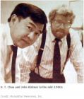
设计创新,提高速度和降低能耗的行业标准的 64 位晶体管内存架构。迅速应用到新的双极逻辑和存储器的设计。 自 1963 TTL ( 1963 里程碑)设备的复杂性,先进的 20 倍,但开关速度保持在每门 10-15 纳秒的延迟相对不变。速度取决于如何快速充电晶体管存储可以去掉。黄金兴奋剂-- 金掺杂 ( 1961 年里程碑)改善,但难以控制。在 1964 年 JR 贝尔德的德州仪器公司( TI )提出使用金属 - 半导体二极管,称为肖特基势垒二极管( 1931 年里程碑) ,分流围绕晶体管的电荷。特德•詹金斯和加思飞兆半导体威尔逊在 1967 年双极型集成电路二极管制造。同时,日本的电工实验室开发出了类似的设计。英特尔设计师理查德•博恩和 H. ţ 蔡氏使用肖特基二极管,在该公司的第一款产品, i3101 64 位的 RAM 的设计。在 1969 年介绍,该装置是较早实现快速的近两倍。 1966 年(里程碑) 在 1971 年 T.I. 推出的 74S 系列 TTL 逻辑系列,采用肖特基二极管,以达到 3 ns 的高速应用的大门延误。低功耗的的肖特基版本,指定的 LS ,迅速取代了原来的 7400 设备,五分之一的电力消耗,提供相同的速度。主席 Mark Shepherd 7400LS 描述为“单一德州仪器的历史中最有利可图的产品线。 ” AMD , Fairchild ,摩托罗拉,国家和 Signetics 也进入了市场。后人,包括 Fairchild 先进的肖特基技术(快速) ,分 2ns 的延迟氧化物隔离工艺相结合的肖特基二极管。 在 70 年代中期,微型可编程位片处理器从 AMD ,英特尔,人机界面,并使用肖特基技术集成 LSI 为高性能运算处理应用的积木 Signetics 公司家庭。 ( 1979 年里程碑) 译者:哈尔滨工业大学(威海)电子封装 090840218赵家玮 原文: http://www.computerhistory.org/semiconductor/timeline/1969-Schottky.html 版权 copyright by www.computerhistory.org The i3101 Schottky TTL 64-bit RAM was Intel's first product 该 i3101 肖特基 TTL64 位内存是英特尔的第一款 Courtesy of: Intel Corporat 74S00 Schottky TTL gate function introduced by TI in 1971 . 74s00 肖特基晶体管晶体管逻辑门功能介绍了钛在 1971 Courtesy of: Texas Instruments, Inc. Introduced in 1975, the Am2901 bit-slice microprocessor used Low-power Schottky (LS) process technology 1975 推出的微处理器, am2901 位片采用低功耗肖特基(镑)工艺技术 Credit: CHM Collection. Gift of John Corbitt Walter Schottky stands between transistor pioneers John Bardeen and Walter Brattain 肖特基•沃尔特站在的先驱约翰巴丁和布拉顿之间 Courtesy of: AIP Emilio Segre Archive, Brattain Collection Since 1963 TTL ( 1963 Milestone ) device complexity had advanced twenty-fold but switching speeds remained relatively unchanged at delays of 10-15 ns per gate. Speed is determined by how quickly charge stored in a transistor can be removed. Gold-doping ( 1961 Milestone ) improved this but was difficult to control. In 1964 J. R. Baird of Texas Instruments (T.I.) proposed using ametal-semiconductor diode, called a Schottky-barrier diode ( 1931 Milestone ), to shunt charge around the transistor. Ted Jenkins and Garth Wilson of Fairchild fabricated such a diode on a bipolar integrated circuit in 1967. Concurrently Japan's Electrotechnical Laboratory developed a similar design. Intel designers Richard Bohn and H. T Chua used a Schottky diode in the design of the company's first product, the i3101 64-bit RAM. Introduced in 1969, the device was nearly twice as fast as earlier implementations. ( 1966 Milestone ) In 1971 T.I. introduced the 74S Series TTL logic family using Schottky diodes to achieve 3 ns gate delays for high-speed applications. Low-power Schottky versions, designated LS, quickly replaced the original 7400 devices by offering the same speed at one fifth the power consumption. Chairman Mark Shepherd described 7400LS as "the single most profitable product line in the history of Texas Instruments." AMD, Fairchild, Motorola, National, and Signetics also entered the market. Later generations, including Fairchild Advanced Schottky Technology (FAST), combined Schottky diodes with oxide-isolation processes for sub-2ns delays. In the mid-1970s micro-programmable "bit-slice" processor families from AMD, Intel, MMI, and Signetics used Schottky technology to integrate LSI building blocks for very high performance arithmetic processing applications. ( 1979 Milestone )
1970 - MOS动态存储器和磁芯存储器相争 约翰 · 施密特设计一个 64 位 p-channel 静态 RAM 在飞兆半导体 (MOS) 在 1964 年。供应商的 1968 萨姆 ( 半导体活跃记忆 ) 项目的十六巴勒斯一般聚集这些芯片在陶瓷基板 , 形成 1024 位混合的数组。整体解决方案和类似的 multi-chip 不久就追上了这个项目在计算机 Microtechnology 、英特尔、摩托罗拉、及 TI(SMA) 。 减少芯片尺寸乔尔 Karp GMe 构思出一种动态的时序方案 Boysel 适应李建造 256 位动态公绵羊在飞兆半导体在 1968 、 1024 和 2048 位装置系统在四个阶段在 1969 年。这些和竞争来自于先进的记忆系统达利克 (AMS6001) 采用晶体管每 4 到 6 点。霍尼韦尔的法案提出了一个 3-transistor 细胞 Regitz 实施 Karp 在英特尔 p-channel 硅门过程 (1968 里程碑 ) 。泰德霍夫提出改进 , 设计了由鲍勃 · 艾博特和调试了鲍勃芦苇于公元 1103 年。提供很多更快的速度 , 标价 1 分 / 一点 , 从 1970 年开始 ,1103 年很快换成了磁性核心技术对计算机内存。沃尔特 Krolikowski 描绘了一幅 Cogar 更快的 n-channel DRAM 于 1970 年。 IBM 是第一个进行这种新的生产工艺技术对系统 1972 年的 370/158 。 Mostek 罗伯特 Proebsting ion-implanted 电阻器用于减少功率消耗及模具尺寸足够装 4 K 位 (MK4096) 进入一个常规 16-pin 包裹于 1973 年。在 16 K(MK4116) 水平在 1976 年 Mostek 采用晶体管单管记忆细胞 , 由 IBM 公司专利的研究员罗伯特 ·Dennard 及设计方法 Karl-Ulrich 斯坦描述西门子。这种做法造成了 64 K 达利克从日本和美国的供应商在最后的十年、大容量的记忆系统 , 半导体 , 更经济可靠比磁芯。 译者:哈尔滨工业大学(威海)电子封装技术 090840219--周明川 校对:哈尔滨工业大学(威海) http://www.computerhistory.org/semiconductor/timeline/1970-DRAM.html 原文: John Schmidt designed a 64-bit MOS p -channel Static RAM at Fairchild in 1964. Fairchild’s 1968 SAM (Semiconductor Active Memory) program for Burroughs assembled sixteen of these chips on ceramic substrates to form 1024-bit hybrid arrays. Monolithic solutions soon overtook this and similar multi-chip projects at Computer Microtechnology, Intel, Motorola, and TI (SMA 2001). To reduce chip size Joel Karp of GMe conceived a dynamic clocking scheme that Lee Boysel adapted to build 256-bit dynamic RAMs at Fairchild in 1968 and 1024 and 2048-bit devices at Four Phase Systems in 1969. These and competing DRAMs from Advanced Memory Systems (AMS6001) employed 4 to 6 transistors per bit. Honeywell’s Bill Regitz proposed a 3-transistor cell that was implemented by Karp in Intel’s p-channel silicon gate process ( 1968 Milestone ). Improvements suggested by Ted Hoff, designed by Bob Abbott and debugged by Bob Reed resulted in the 1103. Offering much faster speed and priced at 1 cent/bit, beginning in 1970 the 1103 quickly replaced magnetic core technology for computer main memory. Walter Krolikowski of Cogar described an even faster n-channel DRAM in 1970. IBM was the first manufacturer to commit to this new process technology on System 370/158 in 1972. Mostek's Robert Proebsting used ion-implanted resistors to reduce power consumption and die size sufficiently to pack 4K bits (MK4096) into a conventional 16-pin package in 1973. At the 16K level (MK4116) in 1976 Mostek adopted the single transistor memory cell patented by IBM researcher Robert Dennard and design methods described by Karl-Ulrich Stein of Siemens. This approach led to 64K DRAMs from Japanese and US vendors before the end of the decade and large capacity semiconductor memory systems that were as reliable as and more economical than magnetic cores. IMG style="FILTER: ; ZOOM: 1; CURSOR: pointer" class=replaced title="Next image " src="http://www.computerhistory.org/semiconductor/assets/images/400x400/1970_1_1.jpg" width=400 height=400 jQuery1331342725637="31" Fairchild 1024-bit SAM multi-chip memory plane uses sixteen 64-bit PMOS Static RAM chips (1968) Credit: Fairchild Camera Instrument Corporation 山姆 multi-chip 供应商 1024 位平面使用内存十六 64 位 PMOS 静态 RAM 芯片 (1968) 贷款 : 照相机和器械企业供应商 IMG style="FILTER: ; ZOOM: 1; CURSOR: pointer" class=replaced title="Next image " src="http://www.computerhistory.org/semiconductor/assets/images/400x400/1970_1_2.jpg" width=400 height=400 jQuery1331342725637="32" IMG style="FILTER: ; ZOOM: 1; CURSOR: pointer" class=replaced title="Next image " src="http://www.computerhistory.org/semiconductor/assets/images/400x400/1970_1_3.jpg" width=400 height=400 jQuery1331342725637="48" IMG style="FILTER: ; ZOOM: 1; CURSOR: pointer" class=replaced title="Next image " src="http://www.computerhistory.org/semiconductor/assets/images/400x400/1970_1_4.jpg" width=400 height=400 jQuery1331342725637="34"
1974 - 通用单片机家族公布于世 一个单芯片的计算机设计的出现乃是 TMS 1000 单片机微单位或一个概念 , 引发了通用数字者家庭权力的工具和发达国家的玩具。 单片机为核心的单元 (MCU) 由相同的基本 ROM 、 RAM 和 CPU 因素以一种微处理器 ( 微控制器 ) 控制要求较低的任务如一个玩具或一个微波炉。这些应用程序不需要的终极速度或程序的复杂性 , 可以实现单片机设计 , 用更少的组件功能齐全适合在一个芯片上。 加里 Boone 和迈克尔的 1971 年《德州仪器的设计 TMS1802 计算机设备提供了基础的单片机为 TMS1000 通用 4 比特 MCU 家庭于 1974 年公布。定价为 $ 2 。在数量上 , 它的动力防盗警报、车库门开启器、游戏、玩具 , 如 “ 讲话和拼写 “ 介绍数码电子给消费者。 在 1976 年 , 两 Mostek 英特尔 (3870) 引入更严格的 8 位的体系结构 , 这种结构服务应用于汽车、电脑外设。英特尔 MCS-48 家庭提供了可擦可编程只读存储器 (8748) 和 (8048)masked-ROM 版本。可编程只读存储器的版本 MCUs 实用了原型与会收取少许生产体系。 (1971 年里程碑 ) 英特尔更加强大 ,1980 年的继任者 ,8051 年 , 成立了一个标准建筑 , 今天在众多变异幸存的具体应用。 到了 1980 年代 MCU 体系结构从欧洲、日本和美国的制造商众多专用应用。服务贝尔实验室的 MAC-4 遇到了电信的需要。摩托罗拉和日立公司从 68000 年 MCUs 派生高性能微处理器。通用设备的家庭照片 ( 今天微芯片 ) 赢的低成本的消费者设计。隐藏在小几百人在电器、汽车、个人电子产品 , 采用单片机可能是当今世界上最无所不在的半导体器件。 译者:哈尔滨工业大学(威海)电子封装 090840222--魏浩 校对:哈尔滨工业大学(威海) http://www.computerhistory.org/semiconductor/timeline/1974-MCU.html 原文: A single-chip calculator design emerges as the TMS 1000 micro-control unit or MCU, a concept that spawned families of general-purpose digital workhorses that power the tools and toys of the developed world. A microcontroller unit (MCU) comprises the same basic ROM, RAM and CPU elements as a microprocessor (MPU) for less demanding tasks such as controlling a toy or a microwave oven. As these applications do not require the ultimate in speed or program complexity, MCU designs can be implemented with fewer components so that the complete function will fit on a single chip. Gary Boone and Michael Cochran’s 1971 design of Texas Instruments TMS1802 single-chip calculator device provided the foundation for the TMS1000 general-purpose 4-bit MCU family announced in 1974. Priced at $2 in volume, it powered burglar alarms, garage door openers, games, and toys such as "Speak and Spell" that introduced digital electronics to the consumer. In 1976 both Intel and Mostek (3870) introduced 8-bit architectures that served more demanding applications in automobiles and PC peripherals. The Intel MCS-48 family offered both EPROM (8748) and masked-ROM (8048) versions. The EPROM version made MCUs practical for prototyping and low-volume production systems. ( 1971 Milestone ) Intel's more powerful 1980 successor, the 8051, established a standard architecture that survives today in numerous variants for specific applications. By the 1980s MCU architectures from European, Japanese and US manufacturers served numerous special-purpose applications. Bell Laboratories’ MAC-4 met telecommunications needs. Motorola and Hitachi derived high-performance MCUs from the 68000 MPU. General Instrument's PIC family (today Microchip) won low-cost consumer designs. Hidden by the hundreds in appliances, automobiles, and personal electronics products, the MCU may be today’s most ubiquitous semiconductor device. IMG style="FILTER: ; ZOOM: 1; CURSOR: pointer" class=replaced title="Next image " src="http://www.computerhistory.org/semiconductor/assets/images/400x400/1974_1_1.jpg" width=400 height=400 jQuery1331346818939="21" An early version of the TMS 1000 microcontroller Courtesy of: Texas Instruments, Inc. 一个早期版本的 TMS 1000 单片机 由 : 德克萨斯仪器公司
IBM 公司的研究员罗伯特 · 迪纳德关于过程缩放型记忆的论文加速了收缩物理尺寸的全球竞赛和制造更复杂的集成电路。 在 60 年代,每个推进光刻能力面具尺寸的线性收缩提供一个快速解决提高速度和降低成本的集成电路。在 1962 年托马斯斯坦利的研究实验室发表的分析指出,由于其临界速度的极限尺寸,栅极长度,躺在横向而不是纵向平面双极器件,这是特别重要的金属氧化物半导体晶体管。 比例原则在布鲁斯卡弗 · 米德 hoeneisen 和加州理工学院的罗伯特迪纳德和他的同事的 1972 个文件被描述。由于登纳德等的 1974 个文件,引起微电子业界的关注与造成的深远影响。他们指出,由于晶体管的横向尺寸的比例系数,因相同的因素速度得到了提高。当时的 绝缘性场效应管 最小尺寸为 5 微米,他们预计缩小微米组分。(人的头发是 50 - 100 微米直径)这是第一次尝试将几何收缩所产生的结果降低功耗和性能改进。这给戈登穆尔( 1965 年)的 “ 定律 ” 提供了科学基础。 1976 年, MITI 组织公司,富士通日立,三菱、东芝,成一个联盟,超大规模集成电路技术研究协会,包括概念,缩放和结合日本光学和精细的制造优势在 70 年代末在全球范围内提供了 64K 动态随机存取存储器( 1970 的里程碑事件)。在这些高能晶体管上计算的功率消耗加快了 互补金属氧化物半导体 管技术的发展( 1963 的里程碑事件)。 这种尺寸 互补金属氧化物半导体 管的能力在 2006 年末允许尺寸收缩至 100 纳米( 0.1 微米)以下和像 IBM 公司 / 索尼 / 东芝的芯片为第三代游戏机提供了 234000000 个晶体管细胞处理器。 80年代中期IBM研究员 罗伯特· 迪纳德 伴随最小特征尺寸内存单元尺寸的减小 100纳米cmos晶体管的扫描电镜图像 第三代游戏机23000000晶体管细胞处理器 译者:哈尔滨工业大学(威海)电子封装090840224-宁尚佳 校对:哈尔滨工业大学(威海)电子封装 090840227-吴喆熹 原文 http://www.computerhistory.org/semiconductor/timeline/1974-Scaling.html 版权 copyright by www.computerhistory.org ———————————————————————————————— 1974 - Scaling of IC Process Design Rules Quantified IBM researcher Robert Dennard’s paper on process scaling on MOS memories accelerates a global race to shrink physical dimensions and manufacture ever more complex integrated circuits. Linear shrinking of mask dimensions with each advance in lithographic capability provided a quick fix to enhance the speed and reduce the cost of ICs in the 1960s. Thomas Stanley of RCA Research Laboratories published an analysis in 1962 noting that this was particularly relevant to the MOS transistor because its critical speed limiting dimension, the length of the gate, lay in the horizontal rather than the vertical plane of bipolar devices. Scaling principles were described in 1972 papers by Bruce Hoeneisen and Carver Mead of Caltech and by IBM's Robert Dennard and his colleagues. But it was a 1974 paper by Dennard, et. al. that caught the attention of the industry with a resulting profound effect on microelectronics. They noted that as the horizontal dimensions of a transistor were scaled by a factor, speed improved by that same factor. At a time when IBM's MOS memories used a minimum dimension of 5 microns, they projected shrinking to fractions of a micron. (A human hair is 50-100 microns in diameter) This was the first attempt to relate a geometry shrink to the resulting power reduction and performance improvement. It gave Gordon Moore's ( 1965 Milestone ) "Law" a scientific foundation. In 1976 MITI organized Hitachi, NEC, Fujitsu, Mitsubishi and Toshiba into a consortium, the VLSI Technology Research Association, that embraced the concept of scaling and combined it with Japanese optical and ultra-clean manufacturing strengths in a global race to deliver 64K DRAMs ( 1970 Milestone ) by the end of the decade. Power consumption at these high transistor counts accelerated the adoption of CMOS technology. ( 1963 Milestone ) The ability to scale CMOS allowed dimensions to shrink below 100 nanometers (0.1 micron) by 2006 and to deliver chips such as the IBM/Sony/Toshiba 234 million transistor Cell processor for the Playstation 3.
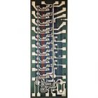
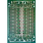
图一 20 世纪 80 年代中期的约翰和 HT 蔡氏 发明单片存储器的约翰和 HT 蔡氏开发了易于使用的可编程阵列逻辑( PAL )和快速原型的定义逻辑功能的设备和工具 创意逻辑设计师意识到,小、快速的 PROM ( 1971 里程碑) ,也可以配置进行简单的逻辑功能。霍尼韦尔要求的基础上,于 1975 年,罗恩·克莱为适合更复杂的逻辑需求适应 Signetics 公司 PROM 电路技术设计了 82S100 可编程逻辑阵列( PLA )。一个所需的功能,表示为布尔逻辑方程,是输入保险丝编程单元,即刻杂设计师的桌面上生成一个定制的 IC 。 约翰和 H.T. 蔡氏与安迪陈在 1978 年推出的一个更精简的架构,他们称为可编程阵列逻辑( PAL ) ,其交易逻辑灵活,有更快的速度和更低的成本。 PALASM ( PAL 汇编)软件设计工具也开发出了易于使用的设备。 License 与 AMD 、国家、 TI 一致将 20 针双极型器件( 16L8 , 16R8 等)确立为行业标准的产品。他们在特雷西基德的一台新机器的灵魂( 1981 年) ,成为一个时代的技术畅销特色。 AMD ( 22V10 )的一个更加灵活的架构 ,来自赛普拉斯和莱迪思的低功率 CMOS 技术,和可重复使用的 CMOS 为基础的 EPROM 器件支持 PC 兼容 Altera 设计原理图输入工具( 1983 年)扩大其应用范围。 赛灵思( 1984 ) ,爱特( 1985 ) , QuickLogic 公司( 1988 )介绍了现场可编程门阵列( FPGA )架构去服务更高的门数的应用。系统设计师选择了统称为 PLD (可编程逻辑器件) ( 1967 里程碑)作为这些用户可配置的首选解决方案超过了所有成本最低或最高性能的应用程序定制的数字逻辑的 ASIC 方法。 图二 MMI PAL16R8 型号的芯片照片 图三 涵盖首次 PAL 应用手册 “ ( 1978 ) 图四 特蕾西基德的普利策奖获奖书 译者:哈尔滨工业大学(威海)电子封装 090840225-石宇辰 校对: 原文 http://www.computerhistory.org/semiconductor/timeline/1978-PAL.html 版权 copyright by www.computerhistory.org ———————————————————————————————— 1978 - PAL User-Programmable Logic Devices Introduced John Birkner and H. T. Chua of Monolithic Memories develop easy-to-use programmable array logic (PAL) devices and tools for fast prototyping custom logic functions. Creative logic designers realized that small, fast PROMs ( 1971 Milestone ) could also be configured to perform simple logic functions. Based on a request from Honeywell, in 1975 Ron Cline adapted Signetics PROM circuit technology to design the 82S100 Programmable Logic Array (PLA) to serve more complex logic needs. A desired function, expressed as set of Boolean logic equations, was entered into a fuse programming unit that instantly generated a custom IC on the designer's desktop. John Birkner and H.T. Chua of Monolithic Memories worked with Andy Chan to introduce a more streamlined architecture they called Programmable Array Logic (PAL) in 1978 that traded logic flexibility for faster speed and lower cost. The PALASM (PAL Assembler) software design tool also made the devices easy to use. License agreements with AMD, National, and TI established the 20-pin bipolar devices (16L8, 16R8, etc) as industry standard products. They are featured in Tracey Kidder’s The Soul of a New Machine (1981), a technology bestseller of the era. A more versatile architecture from AMD (22V10), CMOS technology for lower power from Cypress and Lattice, and reusable CMOS EPROM-based devices supported by PC-compatible schematic-entry design tools from Altera (1983) expanded their range of applications. Xilinx (1984), Actel (1985), and QuickLogic (1988) introduced Field Programmable Gate Array (FPGA) architectures to serve higher gate-count applications. System designers selected one of these user-configurable solutions, collectively known as PLDs (Programmable Logic Devices), over ASIC approaches ( 1967 Milestone ) as the preferred approach to custom digital logic for all but the lowest cost or highest performance application.
贝尔实验室的单芯片DSP-1数字信号处理器设备构架进行了优化,为电子交换系统。 为了能从背景噪声中分离出信息,数字信号处理器( DSP )采用了数学技术来分析来自自然和电子源的模拟信号。转换成数字信号之后,如快速傅立叶变换等算法筛选和重建准备一个可用的模拟信号转换回数据。在音响,通信,图像,雷达,声纳,语音识别系统中,已经实施了 DSP 功能从电子管到集成电路的每一代技术。 在 1970 年,来自 Fairchild 公司( 9334 )和 AMD 公司( 2505 )的 2*4 乘法器作为第一代标准 IC 产品,加快了数学密集型信号处理运算。 TRW 公司的 LSI 产品采用三重扩散双极工艺,建立了更复杂的功能,如 AMD2901 位片在 20 世纪 70 年代后期的视频和国防应用的处理器一起使用的 16x16 乘法器( MPY16 )。 MOS 外围芯片允许信号处理使用通用的微处理器,包括用于摩托罗拉 6800 和英特尔 2920 ( 1979 )的 AMIS2811 ( 1978 ),并结合了可编程的数字信号处理和数据转换电路( 1968 年里程碑)。 单芯片 DSP本质上 是添加了复杂的数学能力的微处理器。贝尔实验室的单芯片 DSP-1 , AT & T 的 ESS 数字交换机的重要组成部分,诞生于 1979 年 5 月。 NEC 的 定点 μ PD7720 ,在 1980 年应用于语音频带,是商业上最成功的早期的 DSP 之一。 TI 的 16 位可编程 DSP 器件的 TMS320 系列从 1983 年开始应用于消费类产品中,从手机到玩具。从 TI 的 集成度更高的 DSP 的连续几代以及 ADI 公司,摩托罗拉,和别人的权力今天的手机,磁盘驱动器, HDTV 产品。 图一: 1979 年贝尔实验室的 DSP-1 设备布局 图二:: 1979 年 TRW 公司的高速乘法累加器的广告 图三::第一的 TMS320 可编程 DSP 器件的芯片的图片 图四::“电子设计”杂志关于 DSP 的专题文章 译者:哈尔滨工业大学(威海)电子封装 090840226-王延博 校对 :哈尔滨工业大学(威海)电子封装 090840216-鞠伯伦 http://www.computerhistory.org/semiconductor/timeline/1979-DSP.html 版权 copyright by www.computerhistory.org 原文 ——————————————————————--------------------------------------------------------------- 1979 - Single Chip Digital Signal Processor Introduced Bell Labs' single-chip DSP-1 Digital Signal Processor device architecture is optimized for electronic switching systems. Digital signal processing (DSP) applies mathematical techniques to analyze analog signals from natural and electronic sources in order to separate information from background noise. After conversion to digital form, algorithms such as the Fast Fourier Transform filter and reconstruct the data ready for conversion back to a useable analog signal. DSP capability has been implemented in every generation of technology from vacuum tubes to ICs in audio, communications, image, radar, sonar, and voice recognition systems. 2 x 4 multipliers from Fairchild (9334) and AMD (2505) in 1970 were among the first standard IC products to speed math-intensive signal-processing algorithms. TRW LSI Products used a triple-diffused bipolar process to build more complex functions, such as the 16x16 multiplier (MPY 16), used together with the AMD 2901 bit-slice processor for video and defense applications in the late-1970s. MOS peripheral chips to enable signal processing using general-purpose MPUs included the AMI S2811 (1978) for the Motorola 6800 and Intel’s 2920 (1979) that combined programmable digital processing and data conversion ( 1968 Milestone ) circuits. Single-chip DSPs are essentially MPUs with added complex math capabilities. Bell Labs’ one-chip DSP-1, a key component of ATT's ESS digital switch, appeared in May 1979. NEC's fixed-point 倀D7720, introduced in 1980 for voiceband applications, was one of the most commercially successful early DSPs. TI’s TMS 320 family of 16-bit programmable DSP devices from 1983 found wide application in consumer products from cell phones to toys. Successive generations of more highly integrated DSPs from TI as well as Analog Devices, Motorola, and others power today's mobile phones, disk drives, and HDTV products.
http://www.springerlink.com/content/vt413114v8v63011/ 最近研究发现呼吸或通过饮水摄取氢气可以中和机体内的活性氧,如羟基自由基,从而通过降低氧化应激诱导的脑、心脏等器官损伤对各种疾病产生保护作用。这些研究认为外源性氢气会与自由基反应,从而被机体“利用”。本研究主要是评价饮用含氢气水后氢气被机体消耗的量。 7 名成年受试者饮用氢气水后,采用气相色谱半导体检测呼吸气体中氢气的含量。呼吸气体中氢气的水平饮水后 10 分钟迅速升高到 36 ppm 。然后迅速在 60 分钟内下降到正常水平,采用呼吸时间和浓度计算出氢气释放的总数量大概为吸收氢气的 59% 。试验过程中氢气的泄露大概 3% 以下。通过皮肤释放的氢气不到 0.1% 。因此大概有 40% 的氢气被保留在身体内。由于氢气属于弱还原剂量,只能和羟基自由基发生中和反应,因此可以推断身体内产生羟自由基的速度低于 1.0 μmol/min/m 2. 这个研究工作没有太多的研究证据,只根据一组人体呼吸气体氢气浓度的检测推断出身体内羟基自由基的产生速度。恐怕太大胆了。 本人提出质疑如下: 一、 氢气还原性弱,只能和羟基自由基反应,但不能排除羟基自由基和其他物质发生反应。氢气进入身体很难和比氢气还原性强的物质进行竞争。因此不能利用氢气被“消耗”的量来判断羟基自由基的产生速度。另外氢气也可能和其他活性强的自由基反应,也不能完全归因于羟基自由基。 二、 氢气摄取和释放应该符合气体运行规律,身体内不同组织溶解和释放氢气的速度完全不同。不同性质的组织溶解氢气的能力也不同。因此难以从整体上分析氢气的保留数量。身体的成分复杂,气体进入身体内,特别是少量气体,很容易被一些分子黏附,这些气体并不是被中和,而是长时间存在于身体内。这类似于把气体通入粘稠的液体中。气体只是物理隔离在液体中而已,并没有被利用。 三、 经过皮肤释放的数量可能不准确。氢气比其他气体分子量小,更容易扩散,更容易经过皮肤扩散。 四、 成年身体内本身存在一定数量的氢气,如何排除干扰。 五、 试验的设计太过简单,例如反复试验多次,看前面保留在身体的氢气是否会影响后来的氢气释放数量。应该设计不同的剂量,看不同剂量的释放和保留是否有规律。 六、 15 年前,有学者曾经用动物试验和氢同位素标记都没有证明氢气被身体利用。而现在采用的技术分辨率远低于同位素标记。竟然说有那么多氢气被利用。别说氢气,许多药物都很难被利用 40% 。而且氢气进入身体只有几分钟时间,更不可能被利用那么多。 总之,这个资料的唯一价值是测定氢气的释放规律。其他的判断和推测近乎荒唐。 Estimation of Molecular Hydrogen Consumption in the Human Whole Body After the Ingestion of Hydrogen-Rich Water Recent studies have revealed that inhaled or ingested hydrogen gas (H 2 ) inactivates reactive oxygen species such as hydroxyl radicals in various kinds of diseases and disorders in animal models and that H 2 reduces oxidative stress-induced damage in brain, heart, and other peripheral tissues. These reports suggested that exogenous H 2 is partially trapped by oxygen radicals. This study was conducted to evaluate H 2 consumption after the ingestion of H 2 -rich water. Seven adult subjects ingested H 2 -rich water. The H 2 content of their expired breath was measured by gas chromatography with a semiconductor. The ingestion of H 2 -rich water rapidly increased breath H 2 content to its maximal level of approximately 36 ppm at 10 min after ingestion and thereafter decreased it to the baseline level within 60 min. Taken together with simultaneous measurements of expiratory minute volume, 59% of the ingested H 2 was exhaled. The loss of H 2 from the water during the experimental procedures accounted for 3% or less of the H 2 . H 2 release from the skin surface was estimated as approximately 0.1%. Based on the remaining H 2 mass balance, approximately 40% of the ingested H 2 was consumed in the body. As the H 2 molecule is reported to be a weak scavenger of hydroxyl radicals and is not effective against superoxide or hydrogen peroxide, the rate of hydroxyl radical production was estimated to be at least 1.0 μmol/min/m 2 (equivalent to 29 nmol/min/kg), assuming that the H 2 molecules were all used to scavenge hydroxyl radicals and that bacterial consumption in the alimentary tract and on the skin surface could be excluded. In summary, 59% of ingested H 2 was exhaled, and most of the remainder was consumed in the body.
有机半导体具有可溶解于溶剂的特殊性质,可以像墨水一样被印刷在柔性的塑性材料上,从而制造出大量的便宜可靠的电路来。但一直以来,有机晶体管的载流子迁移率远远低于Si晶体,使得其应用受到极大的限制。因此如何提高其载流子迁移率成为一个重要课题。 斯坦福大学的 Zhenan Bao 团队,应用了在Si晶体制造工艺中常用的拉伸方法,朝一个方向拉伸有机半导体的晶格并固定下来。实验的结果表明,在特定的拉伸速度下,其载流子迁移率提高成当前最好有机半导体的4倍,这被认为是一个振奋人心的消息,虽然该速率仍仅为Si晶体中的1%,其为有机半导体实现更便宜的印刷电路,可以在显示器方面替代非晶硅(amorphous silicon),以制造更为便宜的3D塑性电视。 该团队采用的有机半导体为 TIPS-pentacene (并五苯),这是一种p型半导体,常规的来讲分子之间距离较远,空穴或电子空位的跳跃较为困难,使得载流子迁移率较低。研究的思路就是将分子聚集得更紧凑一些。最初采用施加张力的拉伸尝试并不能使得分子保持最后的位置,因为有机半导体分子之间的作用力比Si晶体中要弱许多。最后采用的方法,是先将并五苯溶解,维持一定的温度放置在介质的上方,然后用一个板子以特定的角度保持恒定的速率从介质表面一定距离处刷过去,该方法拉伸了分子,并使得溶剂挥发,最后得到了想要的结果和上述性质。 通过拉伸后的光学显微照片如下图所示,可以看到不同的速率会导致不同的薄膜张力和结晶结构(crystalline texture),其中有的结构就可以带来较大的迁移率改善。 Image: Gaurav Giri/Stanford University Quicker Crystals: An optical microscopy image of an organic semiconductor shows that shearing at different speeds caused different crystalline texture and degrees of strain in the film. Just the right amount of strain made charge move a lot faster through the film. Click on image to enlarge.
在晶体中,由于晶格具有周期性,即平移对称性,在单电子近似下,晶态半导体中运动着的电子可以用布洛赫函数来描述,即 ψ k (r)=u k (r)·exp(i k ·r) 其中,u k (r)是具有晶格周期性的函数,k为共有化运动的波矢量。波函数是布洛赫函数意味着电子在晶体各个原胞中出现的几率是相同的,也就是说电子可以在整个晶体内运动。因此,称这时的电子态为 扩展态 ——波函数延伸到整个晶体中。 对于非晶态半导体,由于没有结构上的长程有序性,对运动着的电子势必产生强烈的散射作用,因此,波函数就不再具有布洛赫函数的形式。如果这种散射作用很强,则将发生一种新的现象,即对于某一给定的能量E(这时波矢k已失去了意义),所有的波函数都是定域的(或叫局域的)。其物理图像是每个波函数 ψ E (r)被限制在空间的一个小区域内。 随着距离r的增加,波函数呈指数衰减 。 ψ E (r)~exp(- α·r ) 这种现象是1958年P.W.Anderson在他关于“Absence of Diffusion in Certain Random Lattices”的理论性论文中首先提出来的。因此这种定域化也称为 Anderson定域化 。 若以E m 和E n 分别表示n格点和与n格点最邻近的m格点的原子轨道能量,则能量差值越大,越难实现相邻格点间电子态的转移,亦即越易出现定域态。因此,定域态的是否出现,取决于比值(Em-En)/V(V为相邻格点的交叠积分),比值越大,越有利于定域态的形成。因此,W越大,不同格点上电子态的能量分散程度越大,(Em-En)也越大,顾客认为(Em-En)正比于W。由此可得比值W/V越大,对电子定域态的形成越为有利。Anderson证明,当W/V达到某个临界值(W/V) c 时,整个能带中的所有态都变成定域态。 Mott的进一步研究指出,当无序程度没有达到临界值时,虽然能带中部的态仍保持为扩展态,但在带顶和带底等能带尾部的状态亦可以发生定域化,产生一个有定域态组成的能带尾。Ec与Ec'表示能带中扩展态与尾部定域态的交界处的临界能量。计算结果表明,随着无序程序的增加,定域态与扩展态的交界处向能带中部移动,Ec与Ec'相互接近,最后相遇于能带中部,整个能带中的态都变为定域态。Mott还特别提出, 对于能量在定域态范围的电子,在T=0K时的电子迁移率为0,当能量改变通过Ec或Ec'进入扩展态时,电子迁移率突增至一个有限值 。因此他把能带中扩展态与定域态的交界处Ec和Ec'称作 迁移率边 。在T ≠ 0K时,定域态中的电子可以通过与非晶格子的相互作用而进行跳跃式导电,其迁移率不为零,但与扩散态中的迁移率相比要小得多。因而,当体系的费米能级E F 处于带尾定域态范围时,只有通过热激发从定域态跃迁到迁移率边以上的能带才能产生导电性能,导电性表现为非金属性的。如果由于某种原因使费米能级进入扩展态区,则处于扩展态中的电子将可像金属中电子那样导电,导电性表现为金属性的。这种当费米能级E F 通过迁移率边从定域态进入扩散态的时候发生的从非金属到金属型的导电性的转变称作 Anderson转变 。迁移率边是一个非常重要的概念。但是由实验来观察迁移率边的存在是困难的,只是有些实验可以用迁移率边的假定来加以说明。Mott还进一步认为在迁移率边的金属一边,电导率不是连续地降为零,而是降到一个有限的最小值,称作最小金属化 电导率 σ min 。
 标签: 半导体