第三方供应商发展到具备了半导体结构的专业知识,并且作为技术改进的及关键部分生产设备的供应商出现。 在半导体工业发展的第一个十年,行业推行了 5 种基本结构的晶体管:点接触式晶体管、生长结式晶体管、合金结式晶体管、表面势垒式晶体管和扩散底层式晶体管。 制造商架构起他们自己的生产设施设备投入到每一代产品的制造中。杰克 ·基尔比( 1958 年里程碑式人物)注意到说:“可能我们用到的设备的最贵的那一部分要花费至少 1 万美金 。 由于产品通过平面法( 1959 年的里程碑)向大型化发展,因此出现了产业的和独立的设备制造商,从而将工艺技术也标准化了。制造商专门研究了前端(晶圆加工)和后端(封装、组配和测试)( 1961 年的里程碑)的生产运行。 前端的生产设备,随着晶圆尺寸从 1958 年的 0.5 英寸增大到今天的 12 英寸( 300mm ),其价格也呈数量级增长。早期的前端的生产设备配套供应商包括赛默公司(扩散熔炉)和它旗下的日本电子有限公司、 DW 工业(沉积系统),以及 GCA Mann 和铂金埃尔默公司(光刻设备)( 1955 年的里程碑)。伊智公司, 1961 年费雅嘉分拆出的一个子公司,生产建造了用于晶圆测试的探测设备。 瓦里安公司建造了蒸发器、真空泵和离子注入系统。成立于 1967 年,为制造外延薄膜( 1960 年的里程碑)提供化学气相沉积系统的应用材料公司,通过鼓励半导体供应商将其对制造工艺开发发展工作转交给他们的设备供应商,从而给行业动向带来了改变。 技术工艺的第三方资源,使半导体公司得以关注产品的体系结构及应用,而不再关注于生产和制造工艺的专业知识。这就造成了晶圆代工工厂的兴起,在 19 世纪 80 年代,这些工厂支持了作为新类型的无晶半导体公司的发展。 译者:哈尔滨工业大学(威海)电子封装 090840214葛峰 校对:哈尔滨工业大学(威海)电子封装 090840215申聪敏 原文: http://www.computerhistory.org/semiconductor/timeline/1967-Equipment.html 版权 copyright by www.computerhistory.org 1967 - Turnkey Equipment Suppliers Change Industry Dynamics Third-party vendors develop specialized knowledge of semiconductor fabrication and emerge as vendors of process technology and turnkey manufacturing facilities. During its first decade the semiconductor industry went through five basic transistor structures: point contact, grown junction, alloyed junction, surface barrier, and diffused-base. Manufacturers built their own equipment to support each generation. Jack Kilby ( 1958 Milestone ) noted that "probably the most expensive piece of equipment that we used cost less than $10,000." As production moved to high volumes with the planar process ( 1959 Milestone ), techniques were standardized across the industry and independent equipment producers emerged. Vendors specialized in "Front End" (wafer processing) or “Back End” (package, assembly, and test) ( 1961 Milestone ) operations. Front-end equipment prices increased by orders of magnitude as wafer diameters grew from 0.5 inches in 1958 to today’s 12 inches (300mm). Early front-end tool suppliers include Thermco (diffusion furnaces) and its Japanese licensee Tokyo Electron Ltd, DW Industries (deposition systems), and GCA/Mann and Perkin Elmer (photolithography) ( 1955 Milestone ).Electroglas, a 1961 Fairchild spinout, built probe equipment for wafer testing. In 1965 Kulicke Soffa introduced commercial contact aligners. Varian Associates built evaporators, vacuum pumps, and ion-implantation systems. Founded in 1967 to supply chemical vapor deposition systems for epitaxial films ( 1960 Milestone ), Applied Materials initiated a change in industry dynamics by encouraging semiconductor vendors to shift responsibility for development of manufacturing technology to their equipment suppliers.Third-party sources of technology allowed the semiconductor companies to focus on product architecture and applications rather than process and manufacturing expertise. This led to the rise of "wafer-foundry" vendors who supported a new breed of "fabless" semiconductor companies in the 1980. Michael McNeilly Walter Benzing pioneered epitaxial deposition equipment at Applied Materials, Inc. (应用材料公司倡导外延沉积设备的先驱——迈克尔 ·麦克尼尔,沃尔特·本辛 ) Credit : Semiconductor Equipment and Materials International (SEMI) Applied Materials Model AMV 800 chemical vapor deposition epitaxial reactor (1969) (应用材料公司化学气相沉积外延反应设备 AMV 800 模型) Credit : Applied Materials Technology, Inc Electroglas Model 131B Motorized/Manual Prober allowed testing of die on the wafer before packaging (伊智公司的用于测试封装前晶圆上芯片的自动 / 手动探测器 131B 模型) Credit : Electroglas, Inc Perkin Elmer Micralign projection mask aligner team 1973 ( 1973 年铂金埃尔默公司的 Micralign 投射掩膜对准器团队) Credit : Semiconductor Equipment and Materials International (SEMI)
用自动化设计工具减少开发工程的时间和设计,并提供复杂的定制集成电路 随着英特网共享连接变得复杂化,他们的设计和生产周期延伸到好几年,而一些最终产品寿命周期缩短到一个季度。 1967 年,为了加快美国空军大批量复合定制电路的生产速度, IBM 和德州仪器开发了 “ 自行分配 布线 ” 的方法,采用唯一的一台计算机生成( 1966 年里程碑)每个晶圆金属掩模的技术。 为量产定制设计开发的两种方法是门阵列和标准单元 。他们统称为特定应用集成电路( ASIC )。门阵列是无连接的晶体管的晶片片生产技术。最终定制互连技术确定为最后的生产方案,虽然它比手工制作芯片的硅使用效率低,但是雏形可以从几个月的生产周期缩短为几天。早期门阵列供应商,如费伦蒂 / 协调会是手工的定制连接。 1967 年,飞兆半导体公司在推出微矩阵系列——双极 DTL 和 TTL 电阵列,此阵列可用 CAD 工具来执行两者的相互操作。 1974 年, 罗伯特·利普为国际集成电路设计了第一款 CMOS 阵列,但是可行的 CAD 支持在若干年后也没人设计出来。 标准单元的英特尔网络共享连接采用了一系列应用了装配目录功能设计的制造板罩,并存储在电脑存储信息库中。 他们提供了一个硅高效的手工设计和门阵列的快速掉头之间的折中的方法。 飞兆半导体和摩托罗拉提供的一个早期的 MOS 标准单元权限低于商品牌号 Miscromosaic 和 Polycell 。 超大规模集成电路技术(成立于 1979 年)和 LSI Logic ( 1981 )成功地利用 20 世纪 70 年代被遗弃的 CAD 为基础的 ASIC 概念。当时被摒弃就是因为花费大量的计算时间。 Fairchild 4500 - a 1967 DTL 32-gate Micromatrix custom array designed using CAD tools to interconnect two layers of metal 飞兆半导体 4500 - 1967 年 DTL32 门的 Micromatrix 自定义数组使用 CAD 工具设计,两层金属互连 Credit: Fairchild Camera Instrument Corporation Micromosaic - a 1968 standard cell design for GE Avionics. One of the industry's first designs for revenue micromosaic - 1968 年为 GE 航空电子标准电池的设计。一个行业的第一个设计收入 Credit: Fairchild Camera Instrument Corporation IBM LSI MOD1, an experimental discretionary-wired wafer design by IBM fabricated by Texas Instuments IBM LSI MOD1 , 由 IBM 酌情 - 连接的实验晶片设计由德州自控制作 Credit: International Business Machines Corporation A Ferranti ULA (Uncommitted Logic Array) integrated 14 TTL IC packages for the Sinclair ZX81 PC in 1981 一个费伦蒂 ULA (自由逻辑阵列)集成了 14 组 TTL IC 封装 在 1981 年辛克莱 ZX81 PC Credit: Sinclair Research 1967 - Application Specific Integrated Circuits employ Computer-Aided Design Automated design tools reduce the development engineering time to design and deliver complex custom integrated circuits. As ICs increased in complexity their design and manufacturing turn-around times stretched out to years even as some end product life cycles shrank to a single season. To speed the availability of prototype quantities of complex custom circuits for the Air Force in 1967 IBM and Texas Instruments developed “discretionary-wiring” approaches that employed a unique computer-generated ( 1966 Milestone ) metal mask for every wafer.Two approaches developed for volume production of custom designs are gate arrays and standard cells - collectively known as Application-Specific ICs (ASIC). Gate arrays are produced as wafers of unconnected transistors. As the customizing interconnections are applied at the final manufacturing step, although less efficient in silicon usage than handcrafted chips, prototypes can be produced in days rather than months. Early gate array suppliers such as Ferranti/Interdesign designed the custom connections manually. In 1967 Fairchild introduced the Micromatrix family of bipolar DTL and TTL arrays that used CAD tools to perform this operation interactively. Robert Lipp designed the first CMOS array for International Microcircuits in 1974 but viable CAD support was not forthcoming for several years. Standard cell ICs employ a full set of fabrication masks using designs assembled from catalog functions stored in a computer library.They offer a compromise between silicon-efficient handcrafted designs and the fast turn-around of gate arrays.Fairchild and Motorola offered early MOS standard cell capabilities under the trade names Micromosaic and Polycell. VLSI Technology (founded 1979) and LSI Logic (1981) successfully exploited these CAD-based ASIC concepts abandoned by the original vendors in early 1970s largely due to the then high cost of computing time. 译者:哈尔滨工业大学(威海)电子封装 090840215 申聪敏 校对:哈尔滨工业大学(威海)电子封装 090840214 葛峰 原文: http://www.computerhistory.org/semiconductor/timeline/1967-ASICs.html 版权: copyright by www.computerhistory.org
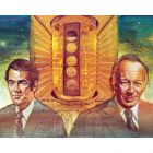
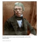
Jack Kilby 图一 杰克 基尔比 Robert Noyce 图二 罗伯特 诺伊斯 一个集成电路由一个单片半导体材料制成,除了晶体管,还包含其他电子元器件。集成电路的发明者是杰克 基尔比和罗伯特 诺伊斯,而罗伯特 诺伊斯去世于1990年。杰克 基尔比于2000年获得了诺贝尔物理学奖。 译者:哈尔滨工业大学(威海)电子封装 070810427-苏琬茹 校对: 原文: http://www.nobelprize.org/educational/physics/transistor/function/ic.html 版权 copyright by www.nobeprize.org ———————————————————————————————— An integrated circuit is made of a single piece of semiconductor material and contains, apart from transistors, other electronical components. The inventors of the integrated circuit were Jack Kilby and Robert Noyce who died in 1990. Jack Kilby was awarded the Nobel Prize in Physics 2000.
1958- 硅台面晶体管进入商业生产 飞兆半导体 生产双扩散硅台面晶体管满足苛刻的航空航天应用 1958 年初,仙童半导体公司以 150 美元从美国联邦系统分部采购 100 晶体管的第一笔订单。 没有既定的生产能满足其 严格规范的 70 车载电脑带有 高压硅晶体管驱动磁芯存储器 。随着 2 个发展项目的推行。戈登穆尔领导的一个小组和吉恩 · 赫尔尼在 pnp 装置中开发了一个 NPN 晶体管和吉恩 · 赫尔尼。 在短短的五个月,创始人(谢尔登罗伯茨)建立的晶形操作( 1956 关),发展光刻掩模技术,使用 16 毫米 movie-camera 镜头(罗伯特诺伊斯),建立了铝所需的特点,为使电气接触(穆尔),并建有自己的生产和试验设备(尤利乌斯空白,胜利格里尼奇,尤金克莱纳)在帕洛阿尔托设施。建筑在暴露于贝尔实验室技术( 1954 关)在肖克利,他们开发了第一个商用双扩散(发射器和基地)硅晶体管,所以命名为其提出的高原样结构。成功后交付的穆尔队的 NPN 晶体管的装置,在 1958 八月介绍了 2n697 型大获好评的惠施康贸易展。 自动控制学为选定的设备使应用在拦截导弹的导航控制系统成为这领域最强的防御。在 1958 年底,一个潜在的可靠性问题使新公司的生存岌岌可危。在金属封装中剥落的微小颗粒对短跨暴露交界处的台地结构产生威胁。 hoerni 的解决方案,著名的平面工艺( 1959 关),彻底改变了工业覆盖暴露有二氧化硅的交界处。 lobby, circa 1960 “ 仙童八 ” 创始人的姿势在公司的大厅,大约 1960 Courtesy of: Wayne Miller, Magnum Photos A B-70 supersonic bomber takes off Credit: U. S. Air Force 70 超音速轰炸机起飞 Fairchild Semiconductor wafer diffusion area, Palo Alto, circa 1958 Credit: Fairchild Camera and Instrument Corporation 飞兆半导体晶 片扩散面积,帕洛阿尔托,大 Detail of a Minuteman I guidance computer Credit: CHM Collection. Gift of Aron Insinga 详细的民兵我制导计算机 译者:哈尔滨工业大学(威海)电子封装 090840122-王孝宝 校对: 王天卓090840121 http://www.computerhistory.org/semiconductor/timeline/1978-PAL.html (原文) 版权 copyright by www.computerhistory.org ———————————————————————————————————— 滨工业大学(威海) 1958 - Silicon Mesa Transistors Enter Commercial Production Fairchild Semiconductor produces double-diffused silicon mesa transistors to meet demanding aerospace applications. In early 1958 Fairchild Semiconductor procured its first order, for 100 transistors at $150 apiece from IBM’s Federal Systems Division. No established manufacturer could meet its exacting specifications for a high-voltage silicon transistor to drive magnetic core memory in the B-70 on-board computer. Two development projects were pursued in parallel. A team led by Gordon Moore developed an n-p-n transistor and by Jean Hoerni, which worked on a p-n-p device. In just five months, the founders ( 1956 Milestone ) set up a crystal-growing operation (Sheldon Roberts), developed photolithographic masking techniques using 16 mm movie-camera lenses (Jay Last, Robert Noyce), established the aluminum characteristics needed for making electrical contacts (Moore), and built their own manufacturing and test equipment (Julius Blank, Victor Grinich, Eugene Kleiner) at their Palo Alto facility. Building on their exposure to Bell Labs techniques ( 1954 Milestone ) at Shockley, they developed the first commercial double-diffused (emitter and base) silicon mesa transistor, so named for its raised plateau-like structure. After successful delivery of the Moore team's n-p-n transistor, the device was introduced as type 2N697 to great acclaim at the Wescon trade show in August 1958. Autonetics selected the device for a guidance-and-control system on the Minuteman ballistic missile, the largest defense program of the era. In late 1958 a potential reliability problem put the new firm’s survival at stake. Tiny particles flaking off the inside of the metal package threatened to short across exposed junctions on the mesa structure. Hoerni's solution, the famous planar process ( 1959 Milestone ), revolutionized the industry by covering the exposed junction with silicon dioxide.
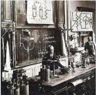
1956- 硅片在硅谷首次出现 肖克利半导体实验室 建造了 加州北部的第一个原型开发半导体设备 来为 硅谷训练年轻的工程师和科学家 。 1955 年 9 月 , 威廉萧克利和阿诺贝克曼同意 建立肖克利半导体实验室作为贝克曼的部门来“积极 、大力开展 关于半导体材料的 活动 ”。肖克利在加利福尼亚州山景城 圣安东尼奥南部道路 租用了 391 号楼,同时,开始招聘“世界上 最有创造力的团队开发、设计、生产晶体管 ”。 他吸引了很 多 能干的工程师和科学家 ,其中 了解和开发硅相关技术和工艺 、 扩散 技术的 戈登 · 摩尔和罗伯特 · 伊斯 都被他招聘来工作。 1956 年 12 月萧克利 因为 发明晶体管获得了诺贝尔物理学奖 ,但是,他的助理开始厌倦了他懒散的管理模式。 他们也觉得公司应该追求更直接生产硅晶体管的机会 而不是期盼遥远的目标“他在实验室将硅应用到电话通讯领域”。 在要求肖克利再雇用一名新的管理后, 摩尔 、 尤利乌斯 · 伊斯 、 格里尼克 、 琼 · 霍尔尼 、 克莱纳 、 拉斯特 、 罗伯茨 8 名 萧克利员工 在 1957 年 9 月 辞职并创立了 美国飞兆半导体公司 在 帕洛阿尔托 。 许多 来自 播实之星的员工 随之而来。 在未来十年 里, 快捷半导体 成长为 在半导体产业最重要的和创新的公司 ,引导了硅谷其他企业科技和文化,其中超微半导体和 英特尔 连接技术,但是,他的公司从来没有获得实际的利润。 贝克曼 在 1960 年 把专利卖给了 Clevite 公司 。 萧克利在斯坦福大学成了一个教授的电气工程与应用科学 的老师。 Toasting Shockley's Nobel Prize award at Rickey's Hotel, Palo Alto, CA. Celebrants include G. Moore, S. Roberts, R. Noyce, and J. Last 肖克利诺贝尔奖奖在里奇的酒店,帕洛阿尔托约礼,包括穆尔,罗伯茨,诺伊斯,和 J · The Shockley Semiconductor Laboratory facility, Mountain View, CA. circa 1960. 肖克利半导体实验室设施,山景,约公元 1960 。 Small-scale silicon zone refining in the Shockley laboratory in Mountain View 小型硅精炼的肖克利实验室在山景 Small-scale silicon zone refining in the Shockley laboratory in Mountain View 小型硅精炼的肖克利实验室在山景 1956 - Silicon Comes to Silicon Valley Shockley Semiconductor Laboratory develops Northern California's first prototype silicon devices while training young engineers and scientists for the future Silicon Valley. In September 1955 William Shockley and Arnold Beckman agreed to found the Shockley Semiconductor Laboratory as a Division of Beckman Instruments "to engage promptly and vigorously in activities related to semiconductors." Shockley rented a building at 391 South San Antonio Road in Mountain View, California, and began recruiting "the most creative team in the world for developing and producing transistors." He attracted extremely capable engineers and scientists, including Gordon Moore and Robert Noyce, who learned about and developed technologies and processes related to silicon and diffusion while working there. In December 1956 Shockley shared the Nobel Prize in Physics for inventing the transistor, but his staff was becoming disenchanted with his difficult management style. They also felt the company should pursue more immediate opportunities for producing silicon transistors rather than the distant promise of a challenging four-layer p-n-p-n diode he had conceived at Bell Labs for telephone switching applications. After unsuccessfully asking Beckman to hire a new manager, eight Shockley employees - including Moore and Noyce plus Julius Blank, Victor Grinich, Jean Hoerni, Eugene Kleiner, Jay Last and Sheldon Roberts - resigned in September 1957 and founded the Fairchild Semiconductor Corporation in Palo Alto. Many other employees, from technicians to PhDs, soon followed. Over the next decade, Fairchild grew into of the most important and innovative companies in the semiconductor industry, laying the technological and cultural foundations of Silicon Valley while spinning off dozens of new high-tech start-ups, including Advanced Micro Devices (AMD) and Intel. Shockley continued pursuing his four-layer diode but his company never realized a profit. Beckman sold the operation to Clevite Corporation in 1960. Shockley became a professor of electrical engineering and applied science at Stanford University. 译者:哈尔滨工业大学(威海)电子封装 090840120-王开伟 校对:哈尔滨工业大学(威海)电子封装 090840117-康志龙
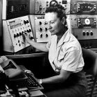
1954 ——硅晶体管提供优越的工作特性 Morris Tanenbaum 在贝尔实验室制造出第一个晶体管,但是第一个把它应用于商业设备制做和销售的是德州仪器的工程师们。 在晶体管存在的前六年,他们一般都是由锗制造出来的。 虽然此元素是比硅更容易得到,并且它支持允许更高频率的操作,但是用它制成的固体器件,在“关”状态下泄漏电流有很大缺陷——那简直是对计算机逻辑的诅咒。 它们也仅限于 0 至 70 ° C 的操作,这也限制了它们在特殊应用程序下的使用。在 杜邦公司开始提供高纯度的半导体级硅材料后,硅器件在 -55 到 125 ° C 条件下使用成为可能 。 在 1954 年 1 月,贝尔实验室的化学家 Morris Tanenbaum 使用摩根·斯巴克斯和戈登·蒂尔的成长交界技术的变化,塑造了第一个硅晶体管。 但是实验室没有在追求它的进一步发展,思考它在商业化生产中的吸引力,这使得几个月后德州仪器( TI )将这一突破性的成果收入囊中。 蒂尔聘请了一队科学家和工程师,离开贝尔实验室在 TI 的组织实验室,由化学家威利斯阿德科克领导研究的硅晶体管。他们采用高纯度杜邦硅,他们的第一个成功的硅晶体管于 1954 年 4 月 14 日制作出来 —— 一个 NPN 结构使用成长结技术。 Tanenbaum 的研究没有了解到的,在 5 月 10 日,俄亥俄州代顿的无线电工程师学会会议提出这一成就,蒂尔由宣布硅晶体管的生产和可供出售创造一个轰动。在 几乎没有竞争的情况下, TI 占据了未来几年的硅晶体管的市场,并取得重大进展直到雷神公司的地位达到成为为世界上最大的商业晶体管的市场供应商。到 20 世纪 50 年代末,硅已成为业界首选的半导体材料。 图一 1954年5月莫顿琼斯的设计出了TI的第一个晶体管的略图 Morton Jones’s May 1954 design sketch of TI's first silicon transistor 图二 1954 TI的 硅晶体团队成员:w .Adcock,mM. Jones, E. Jackson, and J. Thornhill TI's 1954 silicon-transistor team: W. Adcock, M. Jones, E. Jackson, and J. Thornhill 图三 德州仪器公司做的广告强调硅晶体管体积小 Texas Instruments silicon transistor advertising emphasizes small size 图四 莫里斯高(左)与查尔斯丠(右)在贝尔实研室 Morris Tanenbaum (left) and Charles Lee (right) at Bell Labs 译者:哈尔滨工业大学(威海)电子封装 090840116-赵英建 校对:哈尔滨工业大学(威海)电子封装 090840115-刘金鑫 原文 http://www.computerhistory.org/semiconductor/timeline/1954-Silicon.html 版权: 2007 Computer History Museum. All rights reserved. 1401 N. Shoreline Blvd., Mountain View CA 94043 Ph 650-810-1010 ———————————————————————————————— 1954 - Silicon Transistors Offer Superior Operating Characteristics Morris Tanenbaum fabricates the first silicon transistor at Bell Labs but Texas Instruments' engineers build and market the first commercial devices. For the first six years of their existence, transistors had all been made with germanium. Although this element is much easier to work with than silicon and allows higher-frequency operation, solid-state devices made with it have far worse leakage currents in the "off" condition - an anathema for computer logic. They are also restricted to 0 to 70°C operation, which limits their use in rugged applications. Silicon devices that function from -55 to 125°C became possible after Dupont began supplying high-purity "semiconductor-grade" material. In January 1954 Bell Labs chemist Morris Tanenbaum fashioned the first silicon transistor using a variation on Morgan Sparks and Gordon Teal’s grown-junction technique. But the Labs did not pursue the process further, thinking it unattractive for commercial production, which allowed Texas Instruments (TI) to claim credit for this breakthrough several months later. Having left Bell Labs to organize a research lab at TI, Teal hired a team of scientists and engineers led by chemist Willis Adcock to work on silicon transistors. Employing high-purity Dupont silicon, they made their first successful silicon transistor — an n-p-n structure using the grown-junction technique — on April 14, 1954. Unaware of Tanenbaum’s work, Teal presented this achievement on May 10 at an Institute of Radio Engineers conference in Dayton, Ohio, creating a sensation by announcing that silicon transistors were in production and available for sale. With little competition, TI dominated the silicon-transistor market for the next few years and made significant inroads into Raytheon’s position as the largest merchant market supplier of transistors. By the end of the 1950s, silicon had become the industry's preferred semiconductor material.
随着高温扩散的太阳能电池技术不断成熟,Charles Lee和Morris将该技术应用在了高速晶体管的制造中. 在1952年,贝尔实验室的化学家Calvin Fuller阐述了一种将杂质掺入硅和锗中的方法:通过与掺有所需杂质的高温气体接触使得硅和锗中掺入杂质。而且他通过调整曝光时间和温度,能精确地控制引入杂质的数量及其穿透深度,使其精度优于1微米,这种方法远远优于普通的P/N结生长技术。 通过在1954年早期和工程师Daryl Chapin和物理学家Gerald Pearson在一起的工作,Fuller将扩散层的n型硅硼原子制作成晶片,在其表面下方形成了大面积的P/N结。通过对这些P/N结进行光照,他们产生了如OHL在1940年发现的那种来自光电效应的强电流,转换效率达到了6%。贝尔实验室于1954年4月26日发布了这种太阳能单元,并将其称为“太阳能电池”,这种太阳能单元被用于农村的电话系统以及空间卫星中。 在当年晚些时候查理斯•李利用扩散效应在仅仅几微米厚的基板上制作出了晶体管,这些晶体管的频率可被提升到170MHZ----是以往产品的十倍速度。在1955年3月,富勒采用向硅晶片中扩散进两种杂质的办法成功形成了N-P-N夹层,而化学家MORRIS TANENBAUM和他的研究生D.E.THOMAS制成了硅扩散晶体管。在1956年1月贝尔实验室专门针对上述技术和其他扩散技术开发了三极晶体管技术。 One of the first diffused-base silicon transistors at Bell Labs Courtesy of: Morris Tanenbaum 1960年,在Fairchild的扩散炉中的硅晶体管硅片 Calvin Fuller examining early photovoltaic cellscopy; 2006-2007 Alcatel-Lucent. All rights reserved Calvin Fuller研究早期光伏电池 An advertisement for the Bell Solar Battery - circa 1955 贝尔太阳能电池在大约1955年的广告 Silicon transistor wafer diffusion furnaces at Fairchild in 1960Credit: Fairchild Camera Instrument Corporation 第一扩散基硅晶体管在贝尔实验室 译者:哈尔滨工业大学(威海)电子封装 090840117-康志龙 校对:哈尔滨工业大学(威海)090840120-王开伟 原文: 1954 - Diffusion Process Developed for Transistors Following the production of solar cells using high-temperature diffusion methods, Charles Lee and Morris Tanenbaum apply the technique to fabricate high-speed transistors. Beginning in 1952 Bell Labs chemist Calvin Fuller demonstrated how impurities could be introduced into germanium and then silicon by exposing them to high-temperature gases containing desired dopants. By adjusting the time and temperature of exposure, he could precisely control the amount of impurities introduced and their penetration depth to accuracies of better than one micrometer — far better than achievable with grown-junction techniques. Working with engineer Daryl Chapin and physicist Gerald Pearson in early 1954, Fuller diffused a layer of boron atoms into wafers of n-type silicon, forming large-area p-n junctions just beneath the surface. By shining light on these junctions, they generated a strong electric current via the photovoltaic effect discovered by Ohl in 1940, (1940 Milestone) getting energy conversion efficiencies up to 6 percent. Bell Labs announced this solar cell, dubbed the "Solar Battery," on 26 April 1954. By the late 1950s, solar cells were powering rural telephone systems and space satellites. Later that year Charles Lee used diffusion to make transistors with base layers only a micrometer thick; they could operate at frequencies up to 170 MHz - ten times higher than earlier devices. And in March 1955, employing silicon wafers into which Fuller had diffused two different impurities to form a three-layer n-p-n sandwich, chemist Morris Tanenbaum and his technician D. E. Thomas fabricated silicon diffused-base transistors. In January 1956 Bell Labs held a third symposium on transistor technology (1952 Milestone) specifically devoted to these and other diffusion techniques. copyright by www.computerhistory.org
在十九世纪五十年代,半导体设备在数字计算机上逐渐取代了真空管。直到十九世纪六十年代新设备完全晶体管化。 1950年4月,国家统计局的计算机开始工作,它使用了10,500个锗二极管和747个真空管。 在曼彻斯特大学托姆 基尔伯恩 教授手下学习,瑞查德 格瑞斯达尔和道格拉斯韦伯,于1953年11月16号展示了一台晶体管计算机的原型。这台由 卫星试验中心 制造的 48位的机器用了92个点相连的晶体管和550个二极管,装备到 美国埃梯梯 的联合王国的长途电话中继线装备。一代拥有 250个晶体管结 加强版于 1955年完成。MV电子公司制造了具有六个单元结构,同样拥有该结构 Metrovick950已从 1956年在公司内部实行商业推广。 在1954年,JEANH.FELKER领导一个包括工程师JAMES.R.HARRIS的来自贝尔实验室的研究小组为美国空军设计制造了一台全晶体管计算机,称之为TRADIC(晶体管电子计算机),该机包括大约700个 点接触晶体管和10000个二极管。当该试验机型工作在1MHZ的频率下时,功耗仅不到100W。一个更轻的机载版本(飞行版TRADIC)使用了结形晶体管取代了在C-131飞机上用于导航和控制航弹空投的模拟计算机。由WILLIAMPAPIAN领导的来自麻省理工学院林肯实验室的先进技术发展小组的成员在1956年4月使用来自PHILCO公司的高速锗开关晶体管搭建了速度达5MHZ的通用计算机,也就是众所周知的TX-0(晶体管实验性型)。同样在1956年,日本的第一台通用计算机,ETL3型,使用了130个点接触晶体管和1800个二极管。这台机器是由位于东京的电子技术实验室的HiroshiWada领导研发的. The SEAC computer operator's station 图一:东部标准自动计算机操作员的工作台 University of Manchester (UK) "Manchester TC" transistor computer 图二:联合王国曼彻斯特大学“曼彻斯特TC”晶体管计算机 J. H. Felker and J. R. Harris work on the Bell Labs TRADIC computer 图三:JH菲尔克和JR哈瑞斯在贝尔实验室的TRDIC计算机前工作 The RCA 501 computer, one of the first commercial transistorized machines in the U.S., was announced in 1958 图四:RCA 501计算机,美国第一台商业晶体管计算机在1958年面世 译者:哈尔滨工业大学(威海)电子封装 090840115-刘金鑫 校对:哈尔滨工业大学(威海)电子封装 090840116-赵英建 原文 http://www.computerhistory.org/semiconductor/timeline/1953-transistorized-computers-emerge.html 版权 copyright by www.computerhistory.org ———————————————————————————————— 1953 - Transistorized Computers Emerge During the 1950s, semiconductor devices gradually replaced vacuum tubes in digital computers. By 1960 new designs were fully transistorized. Operational in April 1950, the National Bureau of Standards Eastern Automatic Computer (SEAC) employed 10,500 germanium diodes and 747 vacuum tubes. Working under Tom Kilburn at Manchester University, Richard Grimsdale and Douglas Webb, demonstrated a prototype transistorized computer on November 16, 1953. The 48-bit machine used 92 point-contact transistors and 550 diodes fabricated by STC, the UK arm of ITT. An enhanced version with 250 junction transistors was completed in 1955. The Metropolitan Vickers Electrical Company manufactured six units as the Metrovick 950, which they used commercially within the company from 1956. Jean H. Felker led a Bell Labs team including engineer James R. Harris that designed and built a fully transistorized computer dubbed TRADIC (TRAnsistor DIgital Computer) for the U. S. Air Force in 1954. Involving about 700 point-contact transistors and over 10,000 diodes, the prototype operated at 1 MHz while requiring less than 100 watts of power. A lighter airborne version (Flyable TRADIC) using junction transistors replaced an analog computer for navigation and bombing control in a C-131 aircraft. Led by William Papian, in April 1956 members of the Advanced Development Group of MIT Lincoln Labs used fast germanium switching transistors from Philco Corporation to build a 5 MHz general-purpose digital computer known as TX-0 (Transistor Experimental). Also in 1956, Japan’s first transistorized computer, the ETL Mark III, using 130 point-contact transistors and 1800 diodes was built under the direction of Hiroshi Wada at the Electrotechnical Laboratory in Tokyo.
在一个电脑芯片上存在将近一百万的晶体管。甚至于在一些顶级的芯片上会呈现数亿的晶体管。为了能够让更多的晶体管可以很合适的装在和电脑芯片一样大小的东西上,这些晶体管需要十分小才可以满足要求。事实上,今天的晶体管已经发展到可以比人类的一根头发还要小很多倍的地步了。 译者:哈尔滨工业大学(威海)电子封装090330112-张慧颖 校对:哈尔滨工业大学(威海)电子封装090840205-钱政英 原文 http://www.nobelprize.org/educational/physics/transistor/function/small.html 版权 copyright by www.nobeprize.org Inacomputerchiptherecanexitasmanyasamilliontransistors.Insomeofthemostadvancedchipsevenseveralhundredsofmillionsoftransistorsarepresent.Tobeabletofitthatmanytransistorsintosomethingassmallasacomputerchip,theyneedtobeextremelysmall.Infacttoday'stransistorsaremany,manytimessmallerthanevenasinglehumanhair. Copyright copy; Nobel Media AB 2012 晶体管与一根头发的大小比较图
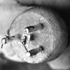
1874 年 半导体点接触整流效应的发现 在半导体二极管的第一份书面说明中,费迪南德·布劳恩指出,电流只在金属与方铅矿接触的那个接触点上自由地流动。 Ferdinand Braun 与 Guglielmo Marconi 共同获得 1909 诺贝尔物理学奖 费迪南德布劳恩在大学在法国斯特拉斯堡担任物理学教授 德国物理学家费迪南德 · 布劳恩 ,柏林大学24岁毕业生,于1874年在 Würzburg 大学研究 了电解质和晶体的导电特点。 当他探索一条晶体(铅硫化 物)方铅矿与点薄的金属丝时,布劳恩指出,电流只在一个方向流动。他发现了在金属与某些晶体材料接触点处的整流效应。 布 劳恩于1876年11月14日在莱比锡向听众 展示这样的半导体器 件,但它并没有发现任何有用的应用,直到无线电的出现,1900年代初期,它也被用于信号探测器在 “ 水晶电台 “ 设置。(1901里程碑) 常见的描述性名称 “ 猫的胡须 ” 探测器来源于用于制造电晶体表面接触的金属微细探针。布劳恩更为人所知的是在1897年发展阴极射线管(CRT)示波器,在德国被称为"百灵管 ” (Braunsche Rohre)。 他与古格列尔莫 · 马可尼共同获得1909年诺贝尔奖,因他们对 “ 无线电报的发展贡献”,主要开发可调谐回路为无线电接收机。 执行整流的电子设备被称为二极管。 1883 年,工作在爱迪生实验室的 William J. Hammer 在给加热丝灯泡补充另一个电极时发现了这种整流效应。 1904年,约翰·弗莱明发明了专利单程 ” 振荡阀",基于所谓的 “ 爱迪生效应 ” ,将交变电流无线电信号转换成耳机或扩音器中的直流电。 今日的二极管,也就是弗莱明阀门,是第一个实用的电子装置。布劳恩的点接触整流二极管执行同样的功能,是使用半导体特性而非热电子特性。 ——————————————————————————————— 译者:哈尔滨工业大学(威海)电子封装 090840102 冯怡 校对:哈尔滨工业大学(威海) 1874 - Semiconductor Point-Contact Rectifier Effect is Discovered In the first written description of a semiconductor diode, Ferdinand Braun notes that current flows freely in only one direction at the contact between a metal point and a galena crystal. Ferdinand Braun shared the 1909 Nobel Prize in Physics with Guglielmo Marconi Credit: www.cathodique.net Ferdinand Braun as a professor of physics at the University of Strasbourg in France Credit: www.cathodique.net German physicist Ferdinand Braun, a 24-year old graduate of the University of Berlin, studied the characteristics of electrolytes and crystals that conduct electricity at Würzburg University in 1874. When he probed a galena crystal (lead sulfide) with the point of a thin metal wire, Braun noted that current flowed freely in one direction only. He had discovered the rectification effect at the point of contact between metals and certain crystal materials. Braun demonstrated this semiconductor device to an audience at Leipzig on November 14, 1876, but it found no useful application until the advent of radio in the early 1900s when it was used as the signal detector in a "crystal radio" set. ( 1901 Milestone ) The common descriptive name "cat’s-whisker" detector is derived from the fine metallic probe used to make electrical contact with the crystal surface. Braun is better known for his development of the cathode ray tube (CRT) oscilloscope in 1897, known as the "Braun tube" (Braunsche R栀爀攀) in German. He shared the 1909 Nobel Prize with Guglielmo Marconi for his "contributions to the development of wireless telegraphy," mainly the development of tunable circuits for radio receivers. Electronic devices that perform rectification are called diodes. Working in Thomas Edison's laboratory in 1883 William J. Hammer noted this rectifier effect when he added another electrode to a heated filament light bulb. In 1904, John Fleming patented a one-way "oscillation valve" based on the, so called, "Edison effect" that converted alternating radio signal currents into direct currents in the earphones or speaker. Known today as a diode, the Fleming valve was the first practical electronic device. The Braun point-contact rectifier diode performs the same function using semiconducting rather than thermionic properties. 原文: http://www.computerhistory.org/semiconductor/timeline/1874-semiconductor.html 版权 copyright by www.computerhistory.org
朱利叶斯 · 利林菲尔德 提交了一项基于硫化铜半导体特征的三极放大器专利,十九 世纪 30 年代 人们一直 试图 制造一个这样的 设备。 波兰 - 美国物理学家 和 发明家朱利叶斯 · E. 利林菲尔德在 1926 年提交 的 专利, “ 用于控制电流的方法和仪器 ” 中,他提出了一个使用硫化铜半导体材料 的 三极结构。如今,这个设备被称为场效应晶体管。 1934 年 在剑桥大学工作 时 ,德国电气工程师和发明家奥斯卡 海尔 提 出了专利,在半导体中 通过电容 性的 耦合 电极控制 电流 - 本质上是一个场效应晶体管。虽然这两个 都 被授予专利, 但 不存在任何记录证明, 海尔 或利林菲尔德 真正制出 运作 的 设备。 1938 年,罗伯特 · 波尔和鲁道夫 Hilsch ,在德国哥廷根大学 ,用三个电极进行 溴钾晶体实验。他们 报道称 放大 了 低频信号(约 1 赫兹),但他们的研究并没 有致予 任何应用。 在贝尔电话实验室关于铜氧化物整流器的研究和 莫特 与 肖特基 关于半导体整流子的解释 ( 1931 里程碑) ,两者的启发下, 威廉 · 肖克利在 1939 年 12 月写道: “ 今 天我意识到,一个放大器 使用半导体,而不是真空 在 原则 上 是可能的。 ” 在他的 带领 下,沃尔特 · 布拉顿和其他 人用这样的 三极装置进行实验,但没有达到放大 作用 。 在战争过后 1945 年 他回到了贝尔实验室 ,肖克利恢复了他 关于 半导体器件 的工作 。他再次未能实现他的预测结果。 1946 年,物理学家约翰 · 巴丁计算 得出 ,表面效应可以解释这些尝试建立 能运行 装置 的失败 。 ( 1947 里程碑) 图 1 JuliusE.Lilienfeld, 护照照片 1926 年 Lilienfeld 专利的所有说明 OskarHeil 和他的妻子,物理学家 AgnesaArsenjewa-Heil ,在意大利 Bormio 1935 年Heil专利的所有说明 译者:哈尔滨工业大学(威海)电子封装 090840104-李涵竹 校对:哈尔滨工业大学(威海) 原文 http://www.computerhistory.org/semiconductor/timeline/1926-field.html 版权 copyright by www.computerhistory.org 英文原文 Julius Lilienfeld files a patent describing a three-electrode amplifying device based on the semiconducting properties of copper sulfide. Attempts to build such a device continue through the 1930s. Polish-American physicist and inventor Julius E. Lilienfeld filed a patent in 1926, "Method and Apparatus for Controlling Electric Currents," in which he proposed a three-electrode structure using copper-sulfide semiconductor material. Today this device would be called a field-effect transistor. While working at Cambridge University in 1934, German electrical engineer and inventor Oskar Heil filed a patent on controlling current flow in a semiconductor via capacitive coupling at an electrode – essentially a field-effect transistor. Although both patents were granted, no records exist to prove that Heil or Lilienfeld actually constructed functioning devices. In 1938 Robert Pohl and Rudolf Hilsch experimented on potassium-bromide crystals with three electrodes at Gottingen University, Germany. They reported amplification of low-frequency (about 1 Hz) signals, but their research did not lead to any applications. Stimulated by research into copper-oxide rectifiers at Bell Telephone Laboratories and by explanations of semiconductor rectification by Mott and Schottky ( 1931 Milestone ), William Shockley wrote in December 1939 that "It has today occurred to me that an amplifier using semi conductors rather than vacuum is in principle possible." Under his direction, Walter Brattain and others performed experiments on such three-electrode devices but did not achieve amplification. On his return to Bell Labs after the war in 1945 Shockley resumed his work on semiconductor devices. Again he failed to achieve his predicted results. In 1946 physicist John Bardeen calculated that surface effects could account for the failure of these attempts to build working devices. ( 1947 Milestone )
艾伦 · 威尔逊使用了量子力学来解释基本的半导体性质。 7 年后,鲍里斯 · 达维多夫(苏联),内维尔莫特(英国),和沃尔特肖特基(德国)各自对整流做出了定义。 德语单词 “ halbleiter ” 翻译成英文为 “ 半导体 ” ,它首次使用是在 1911 年,作为与电导率的金属(导体)和绝缘体之间的材料来描述的。 几十年来科学家们一直没有对半导体的行为作出合理的解释。直到 1931 年,物理学家沃尔夫冈 · 泡利认为, “ 人们不应该继续研究半导体,这是一个肮脏混乱的东西;谁知道是否真的存在半导体。” 在德国莱比锡海森堡研究所工作的那年,剑桥大学的物理学家艾伦 · 威尔逊采纳了费利克斯 · 布洛赫和鲁道夫 · 佩尔斯发现的固体的量子理论来发明了一个半导体行为的模型。在标题为 “ 电子半导体理论”的两个论文中,他提出:“半导体的特殊性能是由于杂质原子的存在或者是因为这种材料的纯晶体”。 1932 年,威尔逊还试图解释在一个点接触整流( 1874 里程碑)中的单向的电流的流动,根据量子力学的隧道,流动是从金属到半导体 - 反之亦然。但是在 20 世纪 30 年代初,随着其他科学家们进行类似的研究中证明出他的解释是错误的。 关于整流的令人满意的解释,终于在 1938 年出现。鲍里斯 · 达维多夫在俄罗斯科学院的 Ioffe 物理技术研究所,列宁格勒、内维尔莫特在英国布里斯托尔大学,沃尔特肖特基在西门子和哈尔斯克在慕尼黑,德国自主的把电子浓度的现象归功于可以设置电流流动的非对称阻隔的 半导体表面。因为 20 世纪 70 年代的同名二极管,肖特基的名字被新一代的技术人员所熟知。 ( 1969 里程碑) A.H。威尔逊(后来被誉为艾伦·威尔逊先生)他在剑桥的日子里。 威尔逊的一个显示杂质含量的能带图草图。 沃尔特肖特基,在弗里茨 - 哈伯研究所,柏林,1953年。 内维尔莫特与弗朗西斯·西蒙(左),大约在1938年。 译者:哈尔滨工业大学(威海)电子封装 090840105-朴晨灵 校对:哈尔滨工业大学(威海)电子封装090840102-冯怡 原文 http://www.computerhistory.org/semiconductor/timeline/1931-The-Theory.html 版权copyrightby www.computerhistory.org Alan Wilson uses quantum mechanics to explain basic semiconductor properties. Seven years later Boris Davydov (USSR), Nevill Mott (UK), and Walter Schottky (Germany) independently explain rectification. Translated into English as "semiconductor," the German word "halbleiter" was first used in 1911 to describe materials with electrical conductivities between those of metals (conductors) and insulators. But a good explanation of semiconductor behavior eluded scientists for decades. As late as 1931, physicist Wolfgang Pauli opined that "one shouldn’t work on semiconductors, that is a filthy mess; who knows whether any semiconductors exist." While working at Werner Heisenberg’s institute in Leipzig, Germany that year, Cambridge University physicist Alan Wilson adapted the quantum theory of solids being developed there by Felix Bloch and Rudolf Peierls to create a model of semiconductor behavior. In two papers titled "The Theory of Electronic Semi-Conductors," he proposed that their peculiar properties were due to the presence of impurity atoms in otherwise pure crystals of these materials. In 1932 Wilson also tried to explain the one-way current flow in a point-contact rectifier ( 1874 Milestone ) as due to quantum-mechanical tunneling from metal to semiconductor - or vice-versa. But along with similar attempts from other scientists in the early 1930s, his explanation eventually proved wrong. Satisfactory explanations of rectification finally emerged in 1938. Boris Davydov at the Ioffe Physico-Technical Institute of the Russian Academy of Sciences, Leningrad, Nevill Mott at Bristol University, England, and Walter Schottky at Siemens and Halske in Munich, Germany independently attributed the phenomenon to a concentration of electrons on the semiconductor surface that set up an asymmetric barrier to current flow. Schottky’s name became familiar to a new generation of technologists through the eponymous diode of the 1970s. ( 1969Milestone )
1940年 pn结的发现 Russell Ohl 发现了 p-n 结和硅中的光电效应,从而引起了结型晶体管和太阳能电池的发展。 Russell Ohl in his laboratory at Bell Laboratories 2006-2007 Alcatel-Lucent. All rights 图一 .Russell Ohl 在贝尔实验室里他自己的实验室中 20 世纪三十年代中期,在美国新泽西州霍姆德尔的贝尔实验室里,一位名为 Russell Ohl 的电化学研究者开始研究硅整流器作为雷达探测器的应用。他发现提高硅的纯度有助于提升它们的探测能力。 1940 年 2 月 23 日 ,他测试的一片硅片表现异常,展示出令人吃惊的结果。当暴露于强光中时,流过硅板的电流轻微地跳动了一下。同时他发现,当用“猫须”探针测试时,晶体的不同部分表现出相反的电场效应。 Ohl 和同事 Jack Scaff 发现硅板上的一个接缝把硅板分成了两个不同的部分,每一部分分别含有不同的杂质。一种杂质是 P 元素,它导致所测样品结构中的电子含量稍微过量;另一种是 B 元素,它导致电子含量略微不足(后来被称为“空穴”)。他们把这两个区域称为 n 型(负极)和 p 型(正极);这两个区域相交的界面或者说“隔阂区”,成为众知的“ p-n 结”。光照射到结上,激发出电子,从 n 极流向 p 极,形成电子流。 Ohl 发现光电效应,给今天的太阳能板( 1954 里程碑)提供了能源。 William Shockley 在 1948 年定义的结型晶体管的概念( 1948 里程碑)就来源于 Ohl 在 1940 年的偶然发现。p -n 结成为了电子产业里最通用的整流器,并且从此成为了半导体器件设计中的一种基本元器件。 Excerpt from Rusell Ohl's notebook entries of February 21, 1940 2006-2007 Alcatel-Lucent. All rights reserved 图二 .Rusell Ohl 在 1940 年 2 月 21 日 的笔记内容的部分摘录 Figures 8 - 13 from Ohl patent filed in 1941 U. S. Patent Office 图三 . 图片 8-13 摘自 Ohl 的收录于 1941 年的专利 同期文献 Ohl,R.S. 《光敏电器》 美国专利 2402662 (收编于 1941 年 5 月 27 日 ,发行于 1946 年 6 月 25 日 )。 Shaff,J.H. Ohl,R.S. 《应用于微波雷达接受器的硅晶体整流器的发展》,贝尔系统工艺期刊, 26 期( 1947 ),第 1 页 口述历史 电气工程师 Ohl,Russel S. 于 1975 年在 Frank Polkinghom 的指引下口述历史。 Frank Polkinghom 是美国新泽西州新不伦瑞克区的罗格斯大学里 IEEE( 译者注:电器和电子工程师协会 ) 成员。 “ Lillian Hoddeson 对 Russell Ohl 的口述历史访问”,( 1976 年 8 月 19-20 )玻尔图书馆及档案馆和美国物理研究所分部的物理学史中心。 更多信息 Riordan,Michael 和 Hoddeson, Lillian ,《 p-n 结的起源》, IEEE 系列( 1997.6 ),页 46-51. Riordan, M 以及 Hoddeson, L. Crystal Fire : 《信息时代的诞生》(纽约: W. W. Norton, 1997 ),页 88-98. Russell Ohl (bow tie) with Jack Scaff (dark hair) at Bell Laboratories Courtesy of: Bell Laboratories and AIP Emilio Segre Visual Archives 图四 . Russell Ohl (蝴蝶结领结)和 Jack Scaff (黑头发)在贝尔实验室 译者:哈尔滨工业大学(威海)电子封装 090840106- 王青 校对:哈尔滨工业大学(威海)电子封装 090840104-李涵竹 原文 http://www.computerhistory.org/semiconductor/timeline/1940-Discovery.html 版权 copyright bywww.computerhistory.org 1940 — p-n 结的发现 Russell Ohl discovers the p-n junction and photovoltaic effects in silicon that lead to the development of junction transistors and solar cells. In the mid-1930s Russell Ohl, an electrochemist at Bell Telephone Labs in Holmdel, NJ, began investigating the use of silicon rectifiers as radar detectors . He found that increasing the silicon purity helped improve their detection ability. On 23 February 1940, he tested a small silicon slab that yielded strange, surprising results. When exposed to bright light, the current flowing through the slab jumped appreciably. He also noticed that different parts of the crystal yielded opposite electrical effects when tested with a " cat’s whisker " style probe. Ohl and colleague Jack Scaff found that a seam in the slab marked the separation of the silicon into regions containing distinct kinds of impurities. One impurity, the element phosphorus, yielded a slight excess of electrons in the sample while the other, boron, led to a slight deficiency (later recognized as "holes"). They called the regions n -type (for negative) and p -type (positive); the surface or "barrier" where these regions met became known as a " p-n junction." Light striking this junction stimulated electrons to flow from the n -side to the p -side, resulting in an electric current. Ohl had discovered the photovoltaic effect that powers today’s solar cells ( 1954 Milestone ). William Shockley’s conception of the junction transistor in 1948 ( 1948 Milestone ) derived from Ohl’s serendipitous 1940 discovery. The p-n junction became the most common form of rectifier used in the electronics industry and has since become a fundamental building block in the design of semiconductor devices. Contemporary Documents Ohl, R.S. "Light-Sensitive Electric Device" U. S. Patent 2402662 (Filed May 27, 1941, Issued June 25, 1946). Shaff, J. H. Ohl, R.S. "Development of silicon crystal rectifiers for microwave radar receivers," Bell System Technical Journal Vol. 26 (1947) p. 1 Oral Histories Ohl, Russel S. Electrical Engineer, an oral history conducted in 1975 by Frank Polkinghorn, IEEE History Center, Rutgers University, New Brunswick, NJ, USA. "Oral history interview of Russell Ohl by Lilllian Hoddeson," (August 19-20, 1976) The Niels Bohr Library Archives and the Center for History of Physics, Divisions of the American Institute of Physics. More Information Riordan, Michael and Hoddeson, Lillian . "The Origins of the pn Junction," IEEE Spectrum (June 1997) pp. 46-51. Riordan, M Hoddeson, L. Crystal Fire: The Birth of the Information Age. (New York: W. W. Norton, 1997 ) pp. 88-98.
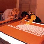
Jules Andrus 和 Walter Bond 应用光刻蚀法技术从印刷工艺到能够在晶圆上精确刻蚀扩散成一个窗口 在 1955 年 Jules Andrus 和 Walter L. Bond 在贝尔实验室 开始把现有的光刻技术(也被称为照相制版)技术开发制造模式应用于印刷电路板使生产更精确, 在硅晶片用到了 更复杂的基于 Frosch 和 Derick’s 二氧化硅层的 设计 。 ( 1955 里程碑)在应用光敏涂料或 “ 抵抗 ” 的层和揭露所需的图案涂层,通过光掩膜,精确的窗口地区被定义在层和化学蚀刻,抵制开幕暴露被冲走。杂质通过这些口扩散到基本硅建立区的 n 型和 p 型硅半导体器件。 1957 年, 在早期的尝试以小型电子电路,杰伊莱斯罗普杰姆斯所有的美国陆军军械引信实验室钻石在马里兰州专利光刻技术用于沉积薄膜的金属条,约 200 微米宽连接离散晶体管的一个陶瓷基板。他们还使用这些技术的蚀刻孔二氧化硅制造二极管阵列。 1959 年, Lathrop 加入了德州仪器,致力于集成电路研究, Nall 去了飞兆半导体。 随后该创举, 1958 年在飞兆半导体公司, Jay Last 和 Robert Noyce 创造了第一个单反相机,应用光刻技术使在一个硅晶片上有很多晶体管。在 1961 年 GCA 的一个分公司 David W. Mann 是第一个公司制作商业步骤,使用重复掩膜来减少设备。 随着特征尺寸低于 0.1 微米变得司空见惯的半导体制造的今天,光刻是一个必不可少的步骤。 译者:哈尔滨工业大学(威海)电子封装-090840119-乔云飞 校对:哈尔滨工业大学(威海)电子封装技术 090840218 赵家玮 原文: http://www.computerhistory.org/semiconductor/timeline/1955-Photolithography.html 版权 copyright by www.computerhistory.org Hand cutting an IC design onto rubylith material for creating the pattern to be optically shrunk onto a photographic mask - early 1970s( 70年代早期, 手工切割 集成电路 设计 ) A completed rubylith layer ready for photographic reduction - circa 1965(一个 完好的 红膜 层显影) Figure from 1957 Lathrop, et al. semiconductor fabrication patent( 图 1957 莱思罗普, 半导体制造 专利 ) Burt Wheeler developed the Mann photorepeater for making masks( 伯特研究出摄影复印机 ) Jules Andrus and Walter Bond adapt photoengraving techniques from printing technology to enable precise etching of diffusion "windows" in silicon wafers. In 1955 Jules Andrus and Walter L. Bond at Bell Labs began adapting existing photolithographic (also called photoengraving) techniques developed for making patterns on printed circuit boards to produce much finer, more intricate designs on silicon in wafers using Frosch and Derick’s silicon-dioxide layer. ( 1955 Milestone ) After applying a photosensitive coating or "resist" on the layer and exposing the desired pattern on this coating through an optical mask, precise window areas were defined in the layer and opened by chemical etching where unexposed resist had been washed away. Impurities were diffused through these openings into the underlying silicon to establish the zones of n -type and p -type silicon needed in semiconductor devices. In an early attempt to miniaturize electronic circuits in 1957, Jay Lathrop and James Nall of the U.S. Army’s Diamond Ordnance Fuse Laboratories in Maryland patented photolithographic techniques used to deposit thin-film metal strips about 200 micrometers wide to connect discrete transistors on a ceramic substrate. They also used these techniques to etch holes in silicon dioxide to fabricate diode arrays. In 1959 Lathrop joined Texas Instruments, working for Jack Kilby, and Nall went to Fairchild Semiconductor. Following up on this pioneering work, Jay Last and Robert Noyce built one of the first "step-and-repeat" cameras at Fairchild in 1958 to make many silicon identical transistors on a single wafer using photolithography. In 1961 the David W. Mann division of GCA Corporation was the first firm to make commercial step and repeat mask reduction devices (photo-repeaters). Photolithography remains an essential step in semiconductor manufacturing today, with feature sizes below 0.1 micrometer becoming commonplace.
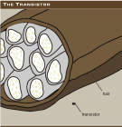
1958年 - 所有半导体固态电路得以证明 杰克.基尔比用半导体材料制造了一个兼有主动与被动部分的微型电路。 随着计算机系统变得更加复杂,工程师们也在寻求更加简单的方法去连接他们所使用的数以万计的晶体管。政府机构资助微型模块和多芯片混合电路工程来解决这个问题。 1952 年,英国电信研究机构的 GWA Dummer 提出“随着晶体管的问世和半导体领域的广泛研究,现在看来可以设想出一种没有连接线的电子设备,并使之封闭于一个固体块中。” 从 50 年代中期到后期,一系列的项目成功地将多个组件集成于一个芯片上。在美国无线电公司, Harwick Johnson 取得了一个无线电振荡器专利, Torkel Wallmark 和 Sanford Marcus 分别创立了移位寄存器和逻辑门。 阿瑟 · 德阿萨罗和伊恩 · 罗斯贝尔实验室制作出了电话应用方面的四阶段计数器。 IBM 公司的乔 · 罗格和里克 · 迪尔制作出了一台使用双基极二极管结构的电脑。日本通产省的 Yasuro Tarui 和德州仪器的 Richard Stewart 提交了多个设备专利。 麻省理工学院的 Dudley Buck 研发了一种超导集成元件制成的低温管。尽管这些成就取得了不同程度的功能,但是没有一个可以解决通用性的系统集成带来的挑战。 1958 年 9 月 12 日,来自德州仪器的 Jack Kilby 在锗基片上用 PNP 型晶体管自己刻蚀制作了一个含有晶体管、电阻、电容等原件的电路。通过使用精致的金制“神奇导线”,他将各自分立的原件连接到了一个振荡电路。一个星期之后,他制作出了放大器。德州仪器在 1959 年 3 月宣布了 Kilby 的“固体电路”概念,并在 1960 年 3 月推出其首个商业设备, 502 型号的二进制触发器,每个售价为 450 美元。但是金线互联并不是一个实用的生产技术。 1961 年 10 月,德州仪器推出的 51 系列直接藕合晶体管逻辑 “ 完全集成电路 ” 系统,使用敷金属平面技术( 1959 年里程碑) 。 图一: Jack Kilby with his lab notebook open at his first solid circuit drawing 杰克 · 基尔比与他的实验室笔记本,展示了他的第一固体电路图纸 Courtesy of: Texas Instruments, Inc 图二: Kilby’s original germanium multi-chip "solid-circuit" oscillator Kilby 的原锗多芯片 “ 固体电路 ” 振荡器 Courtesy of: Texas Instruments, Inc 图三: Connection diagram and open package photograph of the Type 502 flip-flop with "flying-wire" internal connections 连接图和 502 型 “ 飞线 ” 的封装内部连接触发器 Courtesy of: Texas Instruments, Inc 图四: G.W.A. Dummer predicted "solid block" circuits in 1952 G.W.A. dummer 1952 年预测 “ 固体块 ” 电路 Credit: Robert Cathles, under GNU Free Documentation License 译者:哈尔滨工业大学(威海)电子封装 090840123-薛彦峰 校对:哈尔滨工业大学(威海)电子封装 090840125-赵宏博 原文: http://www.computerhistory.org/semiconductor/timeline/1958-Miniaturized.html 版权 copyright by www.computerhistory.org 原文: 1958 - All semiconductor "Solid Circuit" is demonstrated Jack Kilby produces a microcircuit with both active and passive components fabricated from semiconductor material. As computer systems grew more complex, engineers sought simpler ways to interconnect the thousands of transistors they employed. Government agencies funded micro-module and multi-chip hybrid circuit projects in search of a solution to this problem. In 1952, G. W. A. Dummer of England's Telecommunications Research Establishment proposed "With the advent of the transistor and the work in semiconductors generally, it seems now possible to envisage electronic equipment in a solid block with no connecting wires." From the mid to late 1950s several projects succeeded in integrating multiple components on a chip. At RCA Harwick Johnson patented an oscillator and Torkel Wallmark and Sanford Marcus built shift registers and logic gates. Arthur D'Asaro and Ian Ross of Bell Labs fabricated a four-stage counter for telephone applications. Joe Logue and Rick Dill of IBM built a counter using a double-base diode structure. Yasuro Tarui of Japan's MITI and Richard Stewart of TI filed multiple device patents. Dudley Buck of MIT developed the cryotron, an integrated superconducting element. While achieving various degrees of functionality, none of these ideas yielded a solution to the challenge of general-purpose system integration. On September 12, 1958, Jack Kilby of Texas Instruments built a circuit using germanium mesa p-n-p transistor slices he had etched to form transistor, capacitor, and resistor elements. Using fine gold "flying-wires" he connected the separate elements into an oscillator circuit. One week later he demonstrated an amplifier. T.I. announced Kilby's "solid circuit" concept in March 1959 and introduced its first commercial device in March 1960, the Type 502 Binary Flip-Flop priced at $450 each. However the flying-wire interconnections were not a practical production technique. In October 1961, T.I. introduced the Series 51 DCTL "fully-integrated circuit" family using deposited-metal planar technology ( 1959 Milestone ).
 标签: 半导体