2012有机半导体国际研讨会.doc 2012 有机半导体国际研讨会邀请函 2012 年 6 月 3 日 至 6 月 4 日 湖南 长沙 尊敬的老师: 您好! 由国家自然科学基金委支持,中南大学主办的 2012 有机半导体国际研讨会( Organic Semiconductor Workshop 2012 )将于 6 月 3 日 至 4 日在湖南长沙举行 ,议题涵盖 有机发光二极管 ( OLED ) 、有机薄膜晶体管 ( OTFT ) 、有机太阳能电池 ( OPV ) ,有机半导体自旋电子学,有机半导体界面等。 有机半导体材料 (OSC) 近年来已发展为一类具有广阔应用前景的新型功能材料,积极开展对有机半导体材料及其器件的深入研究,对占领该领域的学科前沿和发展国民经济均具有重大的意义。此次国际研讨会邀请了众多国内外有机半导体领域的知名专家学者,旨在交流有机半导体最新进展和今后研究的发展方向,开展国内外同行间的合作,形成高水平的研究成果,提高研究生的培养水平,促进形成高水平的研究团队。 因此,我们诚挚地邀请您和您的同事及研究组成员拔冗光临研讨会并介绍工作成果。如能惠临,敬请使用附件 4 的会议回执,于 5 月 18 日以前发至 osc2012@csu.edu.cn 此致 敬礼! 2012 有机半导体国际研讨会组委会 2012 年 5 月 7 日 附件 1 2012 有机半导体国际研讨会日程和会务 一、会议日程: 1. 2012 年 6 月 2 日 ,嘉宾报到,现场注册。 2. 2012 年 6 月 3 日 ,开幕式、大会邀请报告。 3. 2012 年 6 月 4 日 ,大会邀请报告、各分会场小组专题报告。 4. 2012 年 6 月 5 至 6 日,张家界旅游 二、会务相关事项: 1. 报到地点:枫林宾馆(长沙市岳麓区枫林一路 43 号 ) 2. 会议注册:参加研讨会的注册费为人民币 800 元(研究人员)、 600 元(学生),住宿费、旅游费自理; 3. 大会语言:英语; 4. 墙报要求: 120CM *90CM ,请各位代表按要求自行打印并带至会场,按指定位置张贴; 5. 联系人:高永立(组委会主任 ) 邓宏贵(秘书长 13975159948 ) 张小姣(秘书 13973192264 ) Email: osc2012@csu.edu.cn 附件 2 :已应邀出席研讨会的主要嘉宾 已应邀出席研讨会的主要嘉宾 l 美国: Prof. Ching W. Tang, 美国工程院院士,罗切斯特大学教授,有机半导体发光二极管开创人, 2011 年 Wolf 奖得主; Prof. Franky So, 佛罗里达大学; Prof. Bin Hu, 田纳西大学 ; l 德国: Prof. Martin Aeschlimann, 德国凯泽斯劳滕大学教授,自旋分辨 - 时间分辨双光子能谱专家,德国物理学会表面分会主席; l 加拿大 : Prof. Zheng-Hong Lu, 多伦多大学,加拿大国家教授; l 日本: Prof. Nobuo Ueno; 千叶大学; l 新加坡: Prof. Wei Chen; 新加坡国立大学; l 香港: Prof. C.S. Lee, 香港城市大学,讲座教授 ; l 中国:曹镛院士, 华南理工大学;张泽院士,浙江大学;万立骏院士,中科院化学所;黄维院士,南京邮电大学;刘星元研究员,中科院长春光机所;邱勇教授、帅志刚教授,清华大学;闫东航研究员、马东阁研究员,中科院长春应化所; 廖良生教授,苏州大学;李永舫研究员,中科院化学所; 解士杰教授,山东大学 ; 吴镝教授,南京大学;中科院上海技术物理研究所,戴宁 附件 3 :会议日程总表 2012 有机半导体国际研讨会会议日程 时间 内容 参加人员 地点 6 月 2 日 全天 会议代表报到注册 全体代表 枫林宾馆 6 月 3 日 上午 大会开幕式 合影留念 大会邀请报告 全体代表 枫林宾馆 下午 大会邀请报告 全体代表 枫林宾馆 晚上 欢迎晚宴 全体代表 枫林宾馆 6 月 4 日 上午 大会邀请报告 全体代表 枫林宾馆 下午 小组专题报告 全体代表 中南大学 晚上 墙报及讨论 全体代表 中南大学 6 月 5-6 日 两天 会后考察 代表自愿参加 张家界 附件 4 :参会回执 2012 有机半导体国际研讨会参会回执 大会语言:英语 个人信息 姓 名 职务 / 职称 工作单位 联系电话 Email 报告及墙报情况 是否提供 题目 摘要(请包含题目、主要作者、单位及摘要主体内容。) 是否参加张家界旅游 备注: 1. 报告摘要及墙报内容请包含题目、主要作者、单位及摘要主体内容。 2. 参会住宿地点:枫林宾馆,请您填写住宿天数: 天 3. 回执请发至: osc2012@csu.edu.cn ; 4. 回执请您在 5 月 18 日前返回确认。 附近 5 :部分邀请报告情况 部分邀请报告情况 Invited Speakers Name Organization Country/Region Title Yong Cao South China University of Technology China WATER/ALCOHOL SOLUBLE CONJUGATED POLYMERS FOR INTERFACE MODIFICATION IN POLYMER BULK HETEROJUNCTION SOLAR CELLS Lijun Wan Institute of Chemistry, Chinese Academy of Sciences China Structural detail and property measurement of several typical organic molecule-based nanoarchitecture Ze Zhang Zhejiang University China No Zhigang Shuai Tsinghua University China Electron-phonon couplings in organic semiconductors So Franky University of Florida USA Carrier recombination in polymer solar cells Nobuo UENO Graduate SchoolofAdvancedIntegrationScience,ChibaUniversity Japan Unraveling mysteries in organic semiconductors: Charge mobility and energy level alignment Donghang Yan Changchun Institute of Applied Chemistry China Heterojunction effects and some applications in crystalline organic semiconductors Zhenghong Lu University of Toronto Germany Efficient Droop in OLED Liangsheng Liao Soochow University China Challenges of OLED Technology for Lighting Applications in China Ning Dai Shanghai Institute of Technical Physics, CAS China No Dongge Ma Sate Key Laboratory of Polymer Physics and Chemistry, Changchun Institute of Applied Chemistry, Chinese Academy of Sciences China High efficiency hybrid white OLEDs Shijie Xie School of Physics , Shandong University China Theoretical investigation on organic magnetoresistance based on hyperfine interaction Yongfang Li Institute of Chemistry, Chinese Academy of Sciences China Photovoltaic materials for high efficiency polymer solar cells Wei Chen National University of Singapore Singapore Epitaxial Graphene on SiC: Growth Mechanism and Surface Transfer Doping Xingyuan Liu State Key Laboratory of Luminescence and Applications , Changchun Institute of Optics, Fine Mechanics and Physics, Chinese Academy of Sciences China Electrically pumped organic semiconductor microcavity laser Lingling Wang Hunan University China Magnetic Edge-States in Chiral Graphene Nanoribbon with Reconstructed Edges
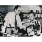
在 威廉 · 肖克利的PN结理论被验证 之后(1948年),制造 一个可以工作的结型晶体管仍然面临严峻的挑战。主要问题是缺乏足够纯净,均匀的半导体材料。贝尔实验室的化学家戈登 · 蒂尔认为,将需要大的单晶,锗和硅, 但听从的人很少,包括 肖克利 。 在管理层很少的支持下, 蒂尔建立自己所需的晶体生长设备, 在 机械工程师约翰小和欧内斯特 · 比埃勒技术员的帮助下。 他在 1917 年由波兰化学家 Jan Czochralski 开发的技术的基础上, 用 一个小的 “ 种子 ” 锗晶体在坩埚熔锗 中 慢慢地缩回来,形成一个狭长的单晶。 肖克利这一成就后来被称为 “ 在初期半导体领域最重要的科学 成果 。 采用这种技术,贝尔实验室的化学家 MorganSparks 通过在 熔融锗晶体生长过程中 加入 微小颗粒杂质,制作 pn 结。 在 1950 年 4 月,他和蒂尔开始向熔体中加入两个连续的小球,第一个是 p 型杂质和第二个是 n 型杂质,形成了内层很薄的 NPN 结构。 一年后,这种 “ 生长出的结型晶体管 ” 超越性能最好的点接触晶体管。 在 1951 年 7 月 4 日, 贝尔实验室在一次 会议 上宣布了这一发现,并强调了肖克利的贡献。 Gordon K. Teal(左)和Morgan Sparks在贝尔实验室,1951年 Morgan Sparks在1949年的第一个结晶体管 2006-2007 Alcatel-Lucent. All rights reserved 1951年,首批微瓦级面结型晶体管中的一只 2006-2007 Alcatel-Lucent. All rights reserve 贝尔M1752型商用结晶体管,约在1951年 Courtesy of: Jack Ward - Transistor Museum 译者:哈尔滨工业大学(威海)电子封装 090840111-计孝智 校对:哈尔滨工业大学(威海)电子封装 090840114-刘继伟 版权 copyright by www.nobeprize.org 原文: http://www.computerhistory.org/semiconductor/timeline/1951-First.html After William Shockley’s theories about p-n junctions had been validated by tests ( 1948 Milestone ), fabricating a working junction transistor still presented formidable challenges. The main problem was lack of sufficiently pure, uniform semiconductor materials. Bell Labs chemist Gordon Teal argued that large, single crystals of germanium and silicon would be required, but few - including Shockley - were listening. With little support from management, Teal built the needed crystal-growing equipment himself, with help from mechanical engineer John Little and technician Ernest Buehler. Based on techniques developed in 1917 by the Polish chemist Jan Czochralski, he suspended a small "seed" crystal of germanium in a crucible of molten germanium and slowly withdrew it, forming a long, narrow, single crystal. Shockley later called this achievement "the most important scientific development in the semiconductor field in the early days." Employing this technique, Bell Labs chemist Morgan Sparks fabricated p-n junctions by dropping tiny pellets of impurities into the molten germanium during the crystal-growing process. In April 1950, he and Teal began adding two successive pellets into the melt, the first with a p- type impurity and the second n- type, forming n-p-n structures with a thin inner, or base, layer. A year later, such “grown-junction transistors” surpassed the best point-contact transistors in performance. Bell Labs announced this advance on July 4, 1951 in a press conference featuring Shockley.
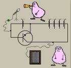
在放大的情况下,晶体管用于放大信号,如声音信号的放大。左边是一个用来放大声音信号的电路的例子。进入麦克风的声音被转换成电信号,这个信号在晶体管中被放大。然后这个被放大的声音信号通过电路,直到它到达扬声器。扬声器将这个声音的电信号重新转换成声音。从音箱中发出的声音与进入麦克风的声音是完全相同的,只是更加响亮了。这就是所谓的放大 - 声音被放大了。 译者:哈尔滨工业大学(威海)电子封装 090840228-谢战胜 校对:哈尔滨工业大学(威海)电子封装 090330112-张慧颖 http://www.computerhistory.org/semiconductor/timeline/ Amplification .html Amplification In the case of amplification the transistor is used to amplify a signal. One example of such a signal can be a sound. To the left is an example of a circuit that is used to amplify sound signals. The sound entering the microphone is converted to an electrical signal that is amplified in the transistor. This amplified sound signal then travels through the circuit until it reaches the loudspeaker. This speaker converts the electrical sound signal back into a sound. The sound leaving the speaker is the same as the sound that entered the microphone, only much louder. This is called amplification – the sound is being amplified. 版权 copyright by www.nobeprize.org 放大
半导体里程 _ 博物馆 _1966- 半导体读写存储器 1966 年 , 半导体读写存储器适用于满足高速存储的需要。因为拥有高性能的存储区和高速缓存的应用,双极性的 RAM 开始进入计算机市场 随机读写存储器储存信息变化频繁因此必须快速存取。到 20 世纪 70 年代中期,由于具有最低的单位存储位成本,磁性铁氧体磁芯阵列占据了随机存储技术的主导地位。 1963 年, Robert Norman 在仙童半导体公司研发取得了半导体静态 RAM 的设计专利。在 1965 年, Scientific Data Systems, Santa Monica, CA and Signetics 几家公司合作开发出了一种全解码的 8 位双极型器件,并且在同年晚些时候元器件工程师 Ben Agusta and Paul Castrucci 开发出了 SP95 ——一种用于 IBM 系统的 16 位的 RAM 。 1966 年, Tom Longo 领导的团队为霍尼韦尔公司 4200 型小型计算机设计的 16 位晶体管逻辑电路高速暂存存储器 TMC3162 成为第一个被广泛使用的半导体 RAM 。仙童公司、西尔瓦尼亚公司、美国德州仪器公司也开始制造这种产品。随后产生的 64 位器件有以下几种: IBM 的缓存芯片、仙童公司的 9035 和 93403 ,因特尔的 3101 ,和德州仪器的 SN7489. 1969 年, IBM 纽约州东费西基尔研究中心为 1971 的装运系统生产出了 128 位的器件—— 370 Model 145 ,这是该公司的第一个商业计算机采用的半导体主存储器。 1970 年 4 月,仙童公司使用 H.T. Chua 设计的 256 位晶体管逻辑电路芯片 4100 ( aka93400 )完成了为宝来公司 Illiac IV 设计的半导体主存储系统。使用 Douglas Peltzer’s Isoplanar 的脱氧过程,能够在提高速度的同时减少硅片的消耗。 1971 年, Bill Herndon 据此设计出了一种快速的 256 位晶体管逻辑电路存储器 93410 。以 Isoplanar 过程为基础,克雷一号超级计算机使用了 65000 个仙童公司生产的 1024 位 ECL RAM 。双极性技术能让计算机速度更快,但是它需要使用 MOS 程序来推广低成本的解决方案以便于主存储器得到广泛的多用途的应用。 译者 : 哈尔滨工业大学 ( 威海 )090840212 高丙欢 校对 : 哈尔滨工业大学 ( 威海 )090840213 邱东阳 http://www.computerhistory.org/semiconductor/timeline/1978- Semiconductor .html 版权 copyright by www.computerhistory.org Metal mask plot for a 16-bit bipolar TTL RAM. Screen image from a 1967 TV documentary 具有16位双极性晶体管逻辑电路读写存储器的金属掩膜图片 拍摄于一部1967年的电视纪录片 128-bit bipolar RAM designed for the IBM System/360 Model 145 main memory is compared to a magnetic core array 为IBM系统设计的128位双极性RAM,主存储器是磁芯阵列 256-bit TTL RAM used in the Illiac IV Processor Element Memory 256位晶体管逻辑电路RAMIlliac IV处理机器件存储器中使用的256位晶体管逻辑电路RAM The Cray 1 supercomputer used 65,000 Fairchild 10415 high-speed 1024-bit ECL chips for main memory 主存储器中含有65000个仙童公司生产的高速1024位ECL芯片 英文原文 1966 - Semiconductor RAMs Serve High-speed Storage Needs Bipolar RAMs enter the computer market for high-performance scratchpad and cache memory applications. Credit: Fairchild Camera Instrument Corporation Random Access Read-Write Memories (RAMs) store information that changes frequently and must be accessed quickly. Offering the lowest cost per storage bit, magnetic ferrite core arrays comprised the dominant RAM technology through the mid-1970s. Robert Norman patented a semiconductor static RAM design at Fairchild in 1963 that was later used by IBM as the Harper cell. In 1965 a cooperative development between Scientific Data Systems , Santa Monica, CA and Signetics produced a fully-decoded 8-bit bipolar device and later that year Components Division engineers Ben Agusta and Paul Castrucci developed the SP95, a 16-bit RAM for the IBM System /360 Model 95 . A team led by Tom Longo at Transitron built the TMC3162 16-bit TTL scratchpad memory for the Honeywell Model 4200 minicomputer in 1966 that became the first widely second sourced semiconductor RAM. Fairchild (9033), Sylvania (SM-80), and TI (SN7481) also manufactured the design. 64-bit devices followed from IBM (cache memory chip), Fairchild (9035 and 93403), Intel (3101), and TI (SN7489) In 1969 the IBM East Fishkill, NY facility produced a 128-bit device for the 1971 shipment of System/370 Model 145, the company's first commercial computer to employ semiconductor main memory. Using the 4100 (aka 93400) 256-bit TTL chip designed by H.T. Chua, Fairchild delivered semiconductor main memory systems for the Burroughs Illiac IV computer in April 1970. Using Douglas Peltzer’s Isoplanar oxide-isolated process that improved speed while consuming less silicon area, Fairchild's Bill Herndon designed a fast 256-bit TTL memory (93410) in 1971. The Cray 1 supercomputer introduced in 1976 used 65,000 Fairchild 1024-bit ECL RAM chips (10415) based on the Isoplanar process Bipolar technology enabled faster computers but it took the MOS process to deliver low-cost solutions for widespread use in main memory and general-purpose applications. ( 1970 Milestone )
IBM的工程师们开发了用以减少研发错误和设计时间的计算机辅助电子设计自动化工具。 当集成电路开始包含几百个门电路和数以千计的晶体管时,他们所支持的计算机已经可以完成加快设计速度和减少设计错误的任务了。这个方法被称作 CAD (计算机辅助设计)或者 EDA (电子设计自动化)。 IBM 在 20 世纪 50 年代末率先开发了在 700 系列电脑文档下运行的 EDA 程序。到了 1966 年, James Koford 和他的同事们在 IBM 纽约州东费西基尔公司用图形显示器采集 STL 混合电路模块( 1964 里程碑事件)的图案,检查他们的错误并自动将信息转换为掩膜模式。在 Koford 加入 Fairchild RD 后他又与 Hugh Mays 、 Ed Jones 及其他同事一起将这项程序应用于单片集成电路。他们的努力创造了逻辑模拟软件( FAIRSIM )、测试程序生成器软件以及门列阵和标准单元布局布线软件( 1967 年里程碑事件),这些为一代又一代的 EDA 工具打下了坚实的基础。 EDA 有两个重要项目源于非主流产业。 20 世纪 60 年代, Larry Nagel 和 Donald Pederson 以及后来的贡献者 Richard Newton 在美国加州大学伯克利分校开发了 SPICE (模拟集成电路重点项目)电路仿真程序。 1979 年,加州理工学院的 Lynn Conway of Xerox 和 Carver Mead 在他们论著的《超大规模集成电路系统导论》中描述的一个新方法揭开了系统设计和芯片设计过程秘密。 20 世纪 80 年代,益华电脑和美国新思科技公司受到在柏克莱加州大学( SIS )、洛杉矶加利福尼亚大学( RSAP )和科罗拉多大学( BOLD )所做调查的激发,开始对综合逻辑系统进行商业化的包装。这些和先进的布局布线技术、逻辑模拟技术以及其他厂商已有的设计核查规则共同使集成电路的设计生产能力能够紧跟设备复杂度不断增加的步伐。 IBM 360/67 仙童公司 1967 年的以大型计算机为运算动力的 CAD 设计系统 图 1 编辑者:费尔柴尔德摄像机仪器公司 掩模草图数字化手绘系统工具 图 2 提供者:因特尔公司 20 世纪 80 年代基于集成电路 CAD 设计系统的工作站 图 3 米德和加威的成就获得了 1981 年的美国电子奖 图 4 译者:哈尔滨工业大学(威海)电子封装 090840213- 邱东阳 校对:哈尔滨工业大学(威海)电子封装 090840229-朱泯西 版权 copyright by www.computerhistory.org 1966 - Computer Aided Design Tools Developed for ICs IBM engineers pioneer computer-aided electronic design automation tools for reducing errors and speeding design time. IBM 360/67 mainframe-powered CAD system at Fairchild in 1967 Credit: Fairchild Camera Instrument Corporation Mask layout drawing hand digitizing system tool Courtesy of: Intel Corporation Workstation-based integrated circuit CAD system 1980s 1981 Electronics Award for Achievement to Conway and Mead As ICs began to incorporate hundreds of gates and thousands of transistors, the computers they enabled were harnessed to speed the design task and eliminate errors. This process is called CAD (Computer Aided Design) or EDA (Electronic Design Automation). IBM pioneered EDA in the late 1950s with documentation of the 700 series computers. By 1966 James Koford and his colleagues at IBM Fishkill were capturing SLT hybrid circuit module ( 1964 Milestone ) designs on graphical displays, checking them for errors and automatically converting the information into mask patterns. After Koford joined Fairchild RD he worked with Hugh Mays, Ed Jones, and others to apply this process to monolithic ICs. Their efforts created logic simulators (FAIRSIM), test program generators, and place and route software for gate arrays and standard cells ( 1967 Milestone ) that laid the ground work for generations of EDA tools. Two important EDA projects originated outside the mainstream of the industry. Larry Nagel and Donald Pederson, with later contributions by Richard Newton, at U.C. Berkeley developed the SPICE (Simulation Program with IC Emphasis) circuit simulation program in the 1960s. A new methodology described in the 1979 Introduction to VLSI Systems by Lynn Conway of Xerox, PARC and Carver Mead of California Institute of Technology demystified the process of chip design for system designers. Commercial logic synthesis packages from Cadence and Synopsys in the 1980s were stimulated by research at U.C. Berkeley (SIS), U.C.L.A. (RASP), and University of Colorado, Boulder (BOLD). These, together with advancements in place and route, logic simulation, and design rule verification from other vendors, allowed IC design productivity to keep pace with increasing device complexity.
 标签: 半导体