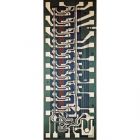
图一仙童公司具有10位模数转换器的电流源-μA722 图二 DAC08 8位输入转换成一个模拟输出 图三单独的双极和CMOS组合包括从1978年年的12位ADCAD574 图四 AD 561和574设计者彼得.霍罗伟 1968 年 - 专用电流源 IC 集成了数据转换功能 将模拟和数字功能结合在一个芯片上制造精度要求,使他们成为众多使用先进单片解决产品问题的厂家之一。 数字是操纵多种信息最有效的形式。然而,现实世界的数据,在本质上是模拟的,必须转换成数字形式进行处理。结合模拟和数字电路的信号,这两种模式之间翻译的集成电路被称为混合信号设备。许多方法被用来完成从模拟到数字(ADC)和数模转换器(DAC)转换,每个方法都需要在不同的精度,速度和成本之间的权衡。 仙童公司的1968年乔治尔德设计的μA722是最早集成电路专用数据转换应用功能的10位电流源之一。在20世纪70年代,许多厂商包括ADI公司,AMD公司,哈里斯,Intersil公司,摩托罗拉,国家半导体,精密整体耐火材料(PMI),德州仪器,和TRW公司开发的家庭设备中的特定部分都集成了数据转换功能。 利用扩散电阻PMI的丹·杜利在1969年设计的第一个完全集成的DAC,6位DAC01。摩托罗拉(MC1408)和PMI(DAC08)随后在1975年的研制了8位器件。由位分辨率表示数据转换器的精度,受制于电阻串的准确性。位分辨率越大,电阻需要的精度越高。在1976年,彼得霍洛威在亚德诺半导体激光通过修剪晶圆薄膜电阻制造的AD561实现了首个单芯片10位DAC的精度要求。使用集成注入逻辑(I2L)双极电路技术,ADI公司的保罗布罗考在1978年设计了第一块单片ADC,10位的AD571。由于ADC比DAC要求更多电路元件,通过双极双芯片和CMOS来解决12位和较高的功能的方案在20世纪80年代初盛行一时。 译者:哈尔滨工业大学(威海)电子封装 090840216-鞠伯伦 校对:哈尔滨工业大学(威海)电子封装 090840226-王延博 原文: http://www.computerhistory.org/semiconductor/timeline/1968-Data.html 版权 copyright by www.computerhistory.org ———————————————————————————————————————— 1968 - Dedicated Current Source IC Integrates a Data Conversion Function The precision manufacturing requirements of combining analog and digital capability on one chip made them one of the last product areas to yield to monolithic solutions. Digital is the most efficient form for manipulating many kinds of information. However, real world data is analog in nature and must be converted to digital form for processing. Integrated circuits incorporating analog and digital circuitry where signals are translated between these two modes are called mixed-signal devices. Numerous approaches are used to accomplish Analog to Digital (ADC) and Digital to Analog (DAC) conversion; each entails different trade offs between accuracy, speed, and cost. Fairchild’s George Erdi designed one of the first ICs dedicated to data conversion applications, the A722 10-bit Current Source, in 1968. In the 1970s many vendors including Analog Devices, AMD, Harris, Intersil, Motorola, National Semiconductor, Precision Monolithics (PMI), TI, and TRW developed families of devices that integrated specific portions of the data conversion function. Using diffused resistors PMI's Dan Dooley designed the first fully integrated DAC, the 6-bit DAC01 in 1969. Motorola (MC1408) and PMI (DAC08) followed with 8-bit devices in 1975. The accuracy of data converters, expressed as bit resolution, is limited by the accuracy of a string of resistors. The larger the bit resolution, the higher the accuracy required of the resistors. In 1976 Peter Holloway at Analog Devices laser trimmed thin-film resistors on the wafers to achieve the required precision for the first single-chip 10-bit DAC, the AD561. Using integrated injection logic (I2L) bipolar circuit techniques, Paul Brokaw of Analog Devices designed the first monolithic ADC, the 10-bit AD571, in 1978. As ADCs require more circuit components than DACs, two-chip bipolar and CMOS solutions prevailed for 12-bit and higher functions through the early 1980s.
1970 - MOS动态存储器和磁芯存储器相争 约翰 · 施密特设计一个 64 位 p-channel 静态 RAM 在飞兆半导体 (MOS) 在 1964 年。供应商的 1968 萨姆 ( 半导体活跃记忆 ) 项目的十六巴勒斯一般聚集这些芯片在陶瓷基板 , 形成 1024 位混合的数组。整体解决方案和类似的 multi-chip 不久就追上了这个项目在计算机 Microtechnology 、英特尔、摩托罗拉、及 TI(SMA) 。 减少芯片尺寸乔尔 Karp GMe 构思出一种动态的时序方案 Boysel 适应李建造 256 位动态公绵羊在飞兆半导体在 1968 、 1024 和 2048 位装置系统在四个阶段在 1969 年。这些和竞争来自于先进的记忆系统达利克 (AMS6001) 采用晶体管每 4 到 6 点。霍尼韦尔的法案提出了一个 3-transistor 细胞 Regitz 实施 Karp 在英特尔 p-channel 硅门过程 (1968 里程碑 ) 。泰德霍夫提出改进 , 设计了由鲍勃 · 艾博特和调试了鲍勃芦苇于公元 1103 年。提供很多更快的速度 , 标价 1 分 / 一点 , 从 1970 年开始 ,1103 年很快换成了磁性核心技术对计算机内存。沃尔特 Krolikowski 描绘了一幅 Cogar 更快的 n-channel DRAM 于 1970 年。 IBM 是第一个进行这种新的生产工艺技术对系统 1972 年的 370/158 。 Mostek 罗伯特 Proebsting ion-implanted 电阻器用于减少功率消耗及模具尺寸足够装 4 K 位 (MK4096) 进入一个常规 16-pin 包裹于 1973 年。在 16 K(MK4116) 水平在 1976 年 Mostek 采用晶体管单管记忆细胞 , 由 IBM 公司专利的研究员罗伯特 ·Dennard 及设计方法 Karl-Ulrich 斯坦描述西门子。这种做法造成了 64 K 达利克从日本和美国的供应商在最后的十年、大容量的记忆系统 , 半导体 , 更经济可靠比磁芯。 译者:哈尔滨工业大学(威海)电子封装技术 090840219--周明川 校对:哈尔滨工业大学(威海) http://www.computerhistory.org/semiconductor/timeline/1970-DRAM.html 原文: John Schmidt designed a 64-bit MOS p -channel Static RAM at Fairchild in 1964. Fairchild’s 1968 SAM (Semiconductor Active Memory) program for Burroughs assembled sixteen of these chips on ceramic substrates to form 1024-bit hybrid arrays. Monolithic solutions soon overtook this and similar multi-chip projects at Computer Microtechnology, Intel, Motorola, and TI (SMA 2001). To reduce chip size Joel Karp of GMe conceived a dynamic clocking scheme that Lee Boysel adapted to build 256-bit dynamic RAMs at Fairchild in 1968 and 1024 and 2048-bit devices at Four Phase Systems in 1969. These and competing DRAMs from Advanced Memory Systems (AMS6001) employed 4 to 6 transistors per bit. Honeywell’s Bill Regitz proposed a 3-transistor cell that was implemented by Karp in Intel’s p-channel silicon gate process ( 1968 Milestone ). Improvements suggested by Ted Hoff, designed by Bob Abbott and debugged by Bob Reed resulted in the 1103. Offering much faster speed and priced at 1 cent/bit, beginning in 1970 the 1103 quickly replaced magnetic core technology for computer main memory. Walter Krolikowski of Cogar described an even faster n-channel DRAM in 1970. IBM was the first manufacturer to commit to this new process technology on System 370/158 in 1972. Mostek's Robert Proebsting used ion-implanted resistors to reduce power consumption and die size sufficiently to pack 4K bits (MK4096) into a conventional 16-pin package in 1973. At the 16K level (MK4116) in 1976 Mostek adopted the single transistor memory cell patented by IBM researcher Robert Dennard and design methods described by Karl-Ulrich Stein of Siemens. This approach led to 64K DRAMs from Japanese and US vendors before the end of the decade and large capacity semiconductor memory systems that were as reliable as and more economical than magnetic cores. IMG style="FILTER: ; ZOOM: 1; CURSOR: pointer" class=replaced title="Next image " src="http://www.computerhistory.org/semiconductor/assets/images/400x400/1970_1_1.jpg" width=400 height=400 jQuery1331342725637="31" Fairchild 1024-bit SAM multi-chip memory plane uses sixteen 64-bit PMOS Static RAM chips (1968) Credit: Fairchild Camera Instrument Corporation 山姆 multi-chip 供应商 1024 位平面使用内存十六 64 位 PMOS 静态 RAM 芯片 (1968) 贷款 : 照相机和器械企业供应商 IMG style="FILTER: ; ZOOM: 1; CURSOR: pointer" class=replaced title="Next image " src="http://www.computerhistory.org/semiconductor/assets/images/400x400/1970_1_2.jpg" width=400 height=400 jQuery1331342725637="32" IMG style="FILTER: ; ZOOM: 1; CURSOR: pointer" class=replaced title="Next image " src="http://www.computerhistory.org/semiconductor/assets/images/400x400/1970_1_3.jpg" width=400 height=400 jQuery1331342725637="48" IMG style="FILTER: ; ZOOM: 1; CURSOR: pointer" class=replaced title="Next image " src="http://www.computerhistory.org/semiconductor/assets/images/400x400/1970_1_4.jpg" width=400 height=400 jQuery1331342725637="34"
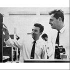
1971 – 将微处理器的功能集成到一个 CPU 芯片上 硅栅 加工与成型技术的产生使得计算机中央处理器 (CPU) 压缩到一块单独的芯片上 在二十世纪六十年代末,设计人员致力于把计算机中央处理器的功能集合到微小的 MOS 大规模集成电路芯片上,这种技术被称为微处理器单元 ( 单片机 ) 芯片集合。 1969 年 Lee Boysel 创造了 Four-Phase 系统有限公司,他在一块半导体上设计植入了早期的八位逻辑算术单元(设计 3800/3804 型)。一个 8 位的 AL-1CPU 片被扩展到了 32 位。在 1970 年 , Garrett AiResearch 的 Steve Geller 和 Ray Holt 设计的 MP944 芯片被用于 F-14A 中央大气数据计算机的芯片,它是被 AMI 公司由六个金属栅晶片组成的。 英特尔的第一个微处理器—— 4004 ,来源于 Ted Hoff 和 Stanley Mazor 的构想。得益于 Masatoshi Shima ,在 1971 年, Federico Faggin 根据 Shima 在硅栅 MOS 芯片技术( 1968 年里程碑式的发展)的经验,将一个由 2300 个晶体管组成的四位微处理器放入到 16-pin 封装起来。 Faggin 指导 Hal Feeney 设计的 8 位 8008 设备于 1972 年公布。为 CTC 公司(即后来的 Datapoint 公司)设计的 8008 设备的原型也曾被德州仪器用于 TMX1795 系统,但是却从没有被用于商业用途。第二代 8 位的设计来源于 Intel ( 设计 8080 型 ) 和 Tom Bennett 在 Motorola 领导的一个团队(设计 6800 型), Tom Bennett 在 1974 年建立被广泛接受的微处理器理念。从 MOS 集成电路技术 -6502 体系衍生出的廉价变种 6800 使得个人电脑和来自于 Apple, Atari, Commodore 或其他公司的游戏可以任意连接。在二十世纪七十年代中期,许多供应商提供增强的 8 位结构,其中 Zilog 公司的最为强大。两个 1975 微处理器预示着后来重要发展趋势,包括在 IBM 工作过的 RCA 的 CMOS COSMAC(1802 里程碑 ) 与 John Cocke 801 精简指令集。 译者:哈尔滨工业大学(威海)电子封装 090840221--马东超 校对:哈尔滨工业大学(威海)电子封装 090840223--吴帅 http://www.computerhistory.org/semiconductor/timeline/1971-MPU.html 版权 copyright by www.computerhistory.org 1971 - Microprocessor Integrates CPU Function onto a Single Chip Silicon-gate process technology and design advances squeeze computer central processing units (CPU) onto single chips. By the late -1960s, designers were striving to integrate the central processing unit (CPU) functions of a computer onto a handful of MOS LSI chips, called microprocessor unit (MPU) chip sets. Building on 8-bit arithmetic logic units (3800/3804) he designed earlier at Fairchild , in 1969 Lee Boysel created the Four-Phase Systems Inc. AL-1 an 8-bit CPU slice that was expandable to 32-bits. In 1970 Steve Geller and Ray Holt of Garrett AiResearch designed the MP944 chip set to implement the F-14A Central Air Data Computer on six metal-gate chips fabricated by AMI. Intel's first microprocessor, the 4004, was conceived by Ted Hoff and Stanley Mazor. Assisted by Masatoshi Shima , Federico Faggin used his experience in silicon-gate MOS technology ( 1968 Milestone ) to squeeze the 2300 transistors of the 4-bit MPU into a 16-pin package in 1971. Faggin also supervised Hal Feeney 's design of the 8-bit 8008 device announced in 1972. Designed for CTC ( later Datapoint ), prototypes of the 8008 function were also built by Texas Instruments as the TMX1795 but never offered commercially. Second generation 8-bit designs from Intel (8080) and from a team led by Tom Bennett at Motorola (6800) in 1974 established widespread acceptance of the MPU concept. A low-cost variant on the 6800 architecture by MOS Technology (6502) enabled personal computers and games from Apple, Atari, Commodore and others. By the mid-1970s many vendors offered enhanced 8-bit architectures, with Zilog 's Z80 being the most enduring. Two 1975 MPUs that presaged important later trends included RCA's CMOS COSMAC 1802 (1963 Milestone ) and John Cocke ’s 801 RISC device at IBM. Beginning in the mid-1970s, 16-bit MPUs emerged from General Instrument (CP1600), National (PACE), TI (TMS9900), and Zilog (Z8000). Boosted by the PC boom of the 1980s, Intel's 8086/8088 (IBM PC) and Motorola's 68000 (Macintosh) devices enjoyed the widest market success. Four Phase Systems, Inc. AL-1 8-bit computer processor slice. Design commenced October 1968. Final working devices March 1969 四相系统,Inc。AL-1 8位计算机处理器片。1968年十月设计开始。1969年三月配置设备。 Gold interconnects highlight the Intel 4004 MPU layout complexity 金色的内连线突出了Intel 4004微处理器复杂的内部构局 The Intel 4004 development team meet again in May 2007. T. Hoff, H. Feeney, S. Mazor, M. Shima, F. Faggin 2007年5月,Intel 4004开发团队合影T. Hoff, H. Feeney, S. Mazor, M. Shima, F. Faggin Internal view of the MCS-4 chip set including the 4004 MPU in the Busicom calculator Busicom 计算机的MCS-4内部图片,设置有4004微处理器
1974 - 通用单片机家族公布于世 一个单芯片的计算机设计的出现乃是 TMS 1000 单片机微单位或一个概念 , 引发了通用数字者家庭权力的工具和发达国家的玩具。 单片机为核心的单元 (MCU) 由相同的基本 ROM 、 RAM 和 CPU 因素以一种微处理器 ( 微控制器 ) 控制要求较低的任务如一个玩具或一个微波炉。这些应用程序不需要的终极速度或程序的复杂性 , 可以实现单片机设计 , 用更少的组件功能齐全适合在一个芯片上。 加里 Boone 和迈克尔的 1971 年《德州仪器的设计 TMS1802 计算机设备提供了基础的单片机为 TMS1000 通用 4 比特 MCU 家庭于 1974 年公布。定价为 $ 2 。在数量上 , 它的动力防盗警报、车库门开启器、游戏、玩具 , 如 “ 讲话和拼写 “ 介绍数码电子给消费者。 在 1976 年 , 两 Mostek 英特尔 (3870) 引入更严格的 8 位的体系结构 , 这种结构服务应用于汽车、电脑外设。英特尔 MCS-48 家庭提供了可擦可编程只读存储器 (8748) 和 (8048)masked-ROM 版本。可编程只读存储器的版本 MCUs 实用了原型与会收取少许生产体系。 (1971 年里程碑 ) 英特尔更加强大 ,1980 年的继任者 ,8051 年 , 成立了一个标准建筑 , 今天在众多变异幸存的具体应用。 到了 1980 年代 MCU 体系结构从欧洲、日本和美国的制造商众多专用应用。服务贝尔实验室的 MAC-4 遇到了电信的需要。摩托罗拉和日立公司从 68000 年 MCUs 派生高性能微处理器。通用设备的家庭照片 ( 今天微芯片 ) 赢的低成本的消费者设计。隐藏在小几百人在电器、汽车、个人电子产品 , 采用单片机可能是当今世界上最无所不在的半导体器件。 译者:哈尔滨工业大学(威海)电子封装 090840222--魏浩 校对:哈尔滨工业大学(威海) http://www.computerhistory.org/semiconductor/timeline/1974-MCU.html 原文: A single-chip calculator design emerges as the TMS 1000 micro-control unit or MCU, a concept that spawned families of general-purpose digital workhorses that power the tools and toys of the developed world. A microcontroller unit (MCU) comprises the same basic ROM, RAM and CPU elements as a microprocessor (MPU) for less demanding tasks such as controlling a toy or a microwave oven. As these applications do not require the ultimate in speed or program complexity, MCU designs can be implemented with fewer components so that the complete function will fit on a single chip. Gary Boone and Michael Cochran’s 1971 design of Texas Instruments TMS1802 single-chip calculator device provided the foundation for the TMS1000 general-purpose 4-bit MCU family announced in 1974. Priced at $2 in volume, it powered burglar alarms, garage door openers, games, and toys such as "Speak and Spell" that introduced digital electronics to the consumer. In 1976 both Intel and Mostek (3870) introduced 8-bit architectures that served more demanding applications in automobiles and PC peripherals. The Intel MCS-48 family offered both EPROM (8748) and masked-ROM (8048) versions. The EPROM version made MCUs practical for prototyping and low-volume production systems. ( 1971 Milestone ) Intel's more powerful 1980 successor, the 8051, established a standard architecture that survives today in numerous variants for specific applications. By the 1980s MCU architectures from European, Japanese and US manufacturers served numerous special-purpose applications. Bell Laboratories’ MAC-4 met telecommunications needs. Motorola and Hitachi derived high-performance MCUs from the 68000 MPU. General Instrument's PIC family (today Microchip) won low-cost consumer designs. Hidden by the hundreds in appliances, automobiles, and personal electronics products, the MCU may be today’s most ubiquitous semiconductor device. IMG style="FILTER: ; ZOOM: 1; CURSOR: pointer" class=replaced title="Next image " src="http://www.computerhistory.org/semiconductor/assets/images/400x400/1974_1_1.jpg" width=400 height=400 jQuery1331346818939="21" An early version of the TMS 1000 microcontroller Courtesy of: Texas Instruments, Inc. 一个早期版本的 TMS 1000 单片机 由 : 德克萨斯仪器公司
 标签: 博物馆