博文
[小资料] 1963年万拉斯(Frank Wanlass)、萨支唐(Chih-Tang Sah)申请的CMOS专利和论文
||
[小资料] 1963年万拉斯(Frank Marion Wanlass)、萨支唐(Chih-Tang Sah)申请的CMOS专利和论文(图片)
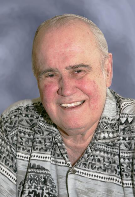
万拉斯 Frank Marion Wanlass, 1933-05-17 ~ 2010-09-09
https://www.invent.org/inductees/frank-wanlass
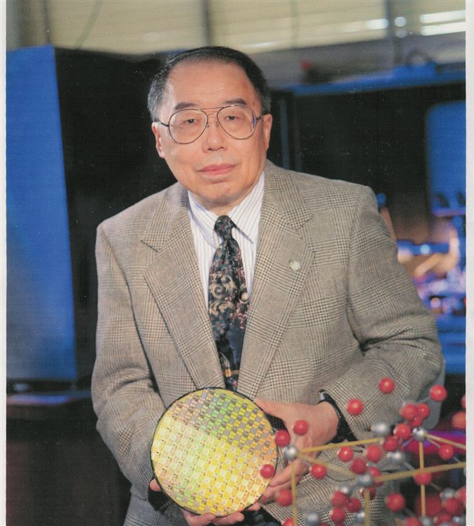
萨支唐 Chih-Tang Sah, 1932-11-10 ~
https://so1.360tres.com/t01faba5d9f4cfe59d5.jpg
https://baike.so.com/doc/5613467-5826077.html
一、人类生产的 1022 个晶体管,其中 99.9% 是 MOS器件
阿塔拉(Martin (John) Mohamed Atalla)、江大原(Dawon Kahng)首先研制出MOS场效应晶体管。
在此基础上,1963年万拉斯(Frank Marion Wanlass)、萨支唐(Chih-Tang Sah)发明的 CMOS,在待机模式下接近零功率。CMOS 电路的第一个大批量应用出现在电池驱动的消费类产品中,如数字手表(1974 Milestone)和不要求最高速度的便携式仪器。
In a 1963 conference paper C. T. Sah and Frank Wanlass of the Fairchild R & D Laboratory showed that logic circuits combining p-channel and n-channel MOS transistors in a complementary symmetry circuit configuration drew close to zero power in standby mode. Wanlass patented the idea that today is called CMOS.
在1963年的一篇会议论文中,仙童研发实验室的 C.T.Sah 和 Frank Wanlass 表明,在互补对称电路配置中结合 p 沟道和 n 沟道 MOS 晶体管的逻辑电路在待机模式下接近零功率。Wanlass 为今天被称为 CMOS 的想法申请了专利。
https://www.computerhistory.org/siliconengine/complementary-mos-circuit-configuration-is-invented/
Wanlass wasn’t interested in studying or analyzing the characteristics of the MOS process. He wanted to fabricate discrete MOSFETs, build ICs with MOSFETs, and design system-level circuits using those devices to nurture demand for the components. Over the next year, he did exactly that. In less than six months, Wanlass designed and fabricated individual p- and n-channel MOSFETs in silicon using the planar process. All the p-channel devices exhibited severe parametric drift, while none of the n-channel devices worked at all. He tested the parametric drift of p-channel devices by putting them in a curve tracer and heating them with a cigarette lighter. He then designed and fabricated a flip-flop IC using MOSFETs and achieved an incredible wafer yield of better than 80%. He developed application circuits for MOSFETs including a current meter that exploited the MOSFET’s extremely high input impedance.
Wanlass 对研究或分析 MOS 工艺的特性不感兴趣。他想制造分立的 MOSFET,用MOSFET 制造 IC,并使用这些器件设计系统级电路,以满足对组件的需求。在接下来的一年里,他确实做到了。在不到六个月的时间里,Wanlass使用平面工艺在硅中设计和制造了单独的 p 沟道和 n 沟道 MOSFET。所有的 p 沟道器件都表现出严重的参数漂移,而没有一个 n 沟道器件工作。他将 p 沟道器件放入曲线示踪剂中,并用打火机加热,从而测试了它们的参数漂移。然后,他设计并制造了一个使用 MOSFET 的触发器 IC,并实现了超过 80% 的令人难以置信的晶圆产量。他开发了 MOSFET 的应用电路,包括一个利用 MOSFET 极高输入阻抗的电流表。
Along the way, Wanlass and his manager C.T. Sah patented the idea for CMOS circuits, which combine p- and n-channel MOSFETs on one silicon die. CMOS is the foundational transistor technology for nearly every IC now manufactured. (Note: Sah is often listed as the sole inventor of CMOS, but his name is on the patent because he was Wanlass’s manager, and it was customary to list the manager along with the inventor on the patent application.)
沿着这个路线,Wanlass 和他的经理 C.T.Sah 为 CMOS 电路的想法申请了专利,该电路将 p 沟道和 n 沟道 MOSFET 结合在一个硅芯片上。CMOS 是目前几乎所有 IC 的基础晶体管技术。(注:Sah 经常被列为 CMOS 的唯一发明人,但他的名字出现在专利上,因为他是 Wanlass 的经理,而且按照惯例,在专利申请中会将经理与发明人一起列出。)
Five decades later the industry had shipped 13 sextillion transistors, 99.9 percent of them MOS devices. And the total increases by multiple billions every day.
【截止到2018年】50年后,该行业已经向市场供应了 1.3×10²² 个晶体管,其中 99.9% 是 MOS器件。总的来说,每天都在以几十亿个的速度增长。
二、1963年万拉斯(Frank Marion Wanlass)、萨支唐(Chih-Tang Sah)发表的会议论文《Nanowatt logic using field-effect metal-oxide semiconductor triodes 使用场效应金属氧化物半导体三极管的纳瓦逻辑》
https://ieeexplore.ieee.org/document/1157450
在 1963-02-20 下午,在会议“1963 IEEE International Solid-State Circuits Conference”上,他们宣读了论文“Nanowatt logic using field-effect metal-oxide semiconductor triodes 使用场效应金属氧化物半导体三极管的纳瓦逻辑”。
图片形式如下:
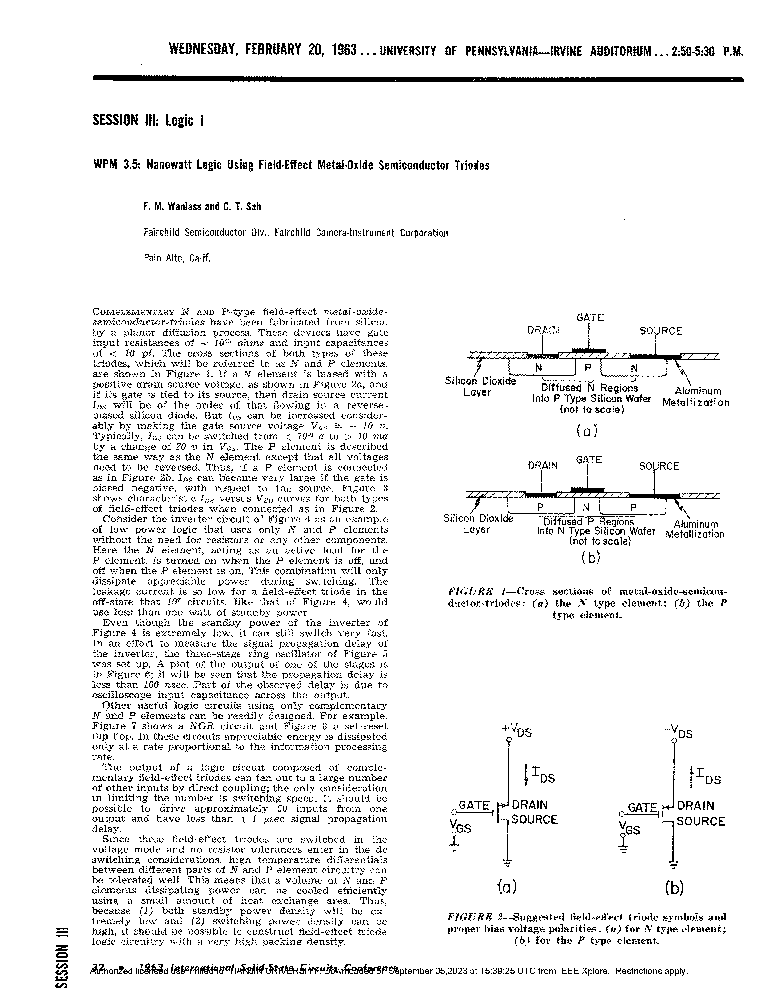
(1)
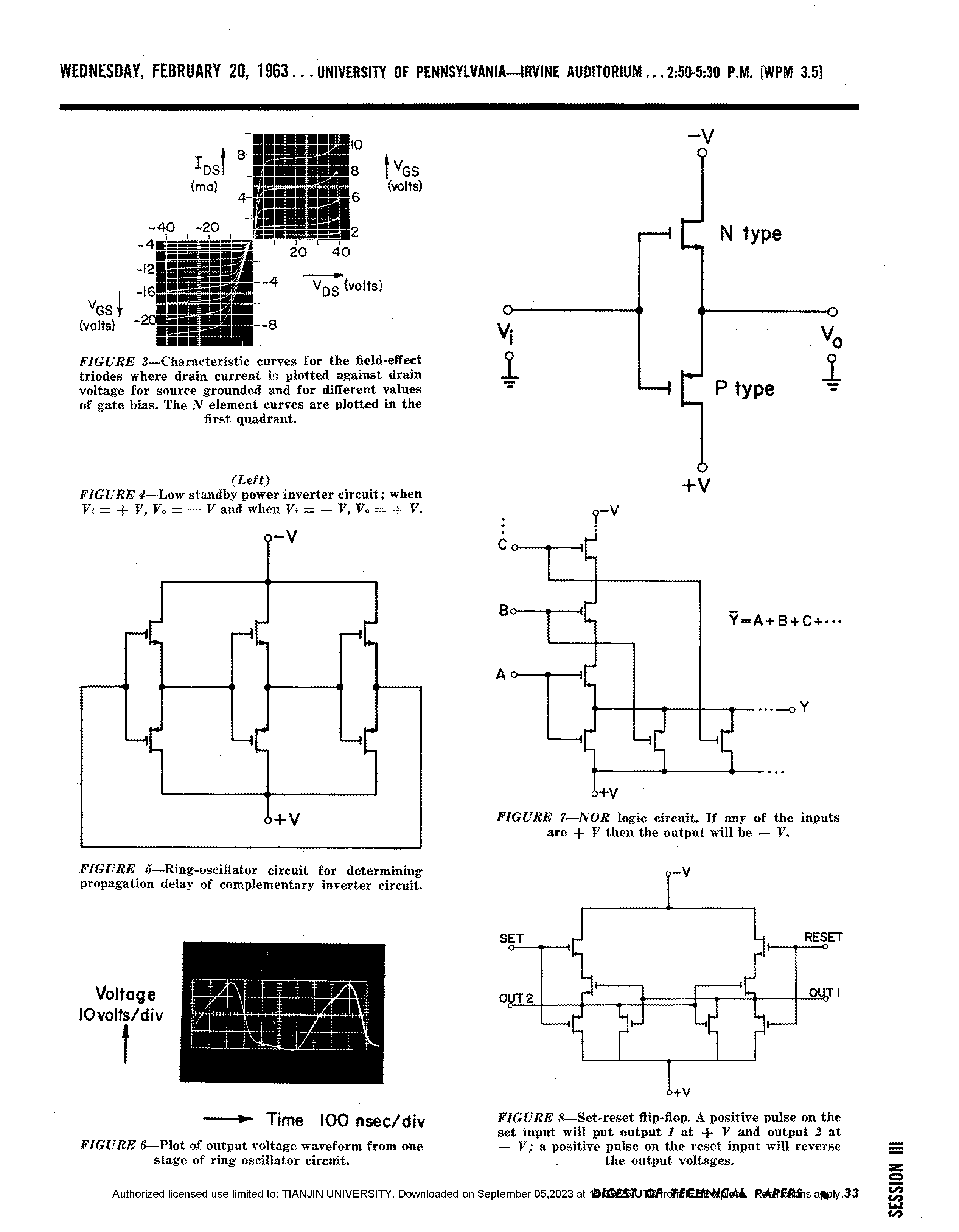
(2)
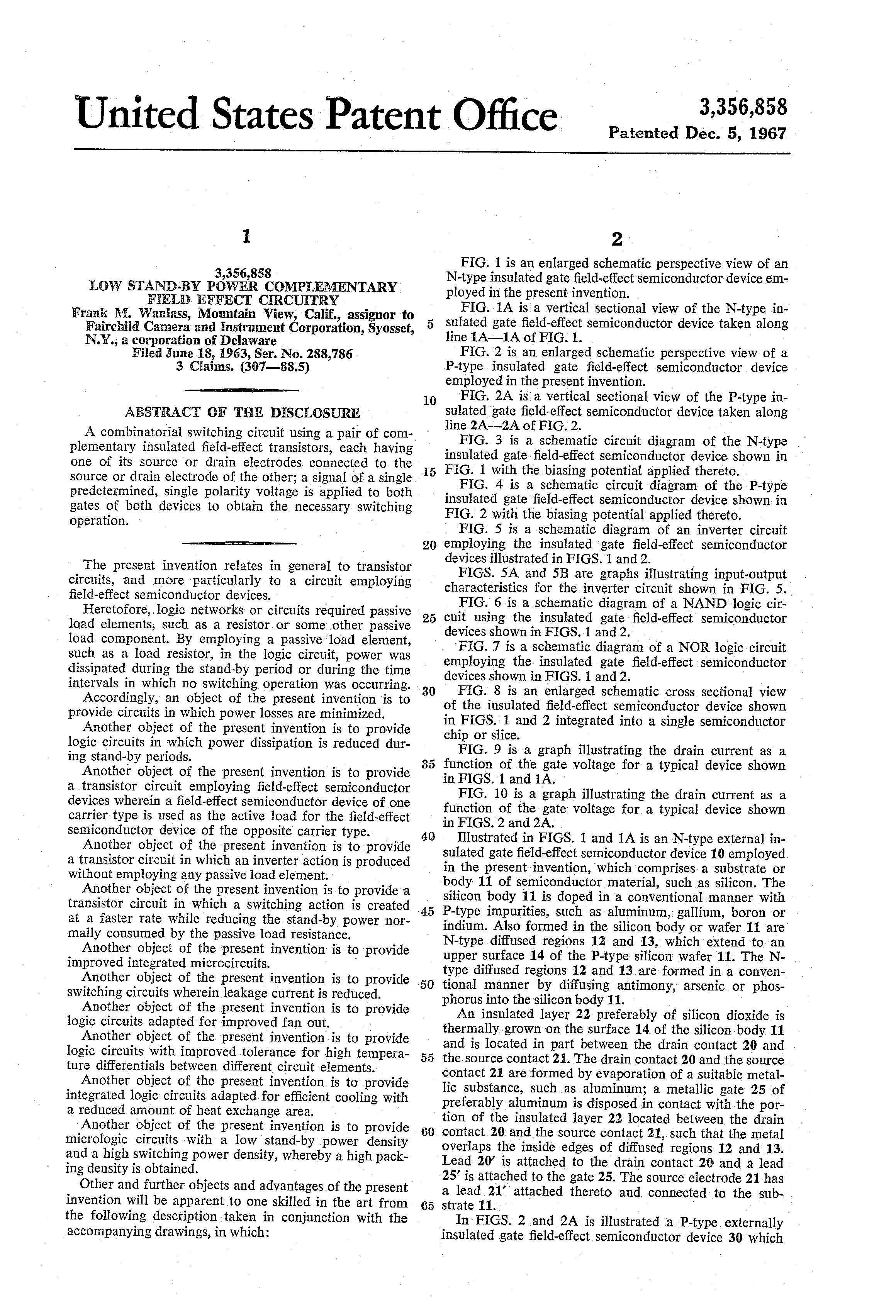
三、1963年万拉斯(Frank Marion Wanlass)、萨支唐(Chih-Tang Sah)申请的美国专利《Low Stand-By Power Complementary Field Effect Circuitry 低待机功率互补场效应电路》
https://image-ppubs.uspto.gov/dirsearch-public/print/downloadPdf/3356858
他们 1963-06-18 申请,1967-12-05 授权的发明CMOS的美国专利《Low Stand-By Power Complementary Field Effect Circuitry 低待机功率互补场效应电路》(U.S. Patent 3,356,858; Filed Dec. 18, 1967):
图片形式如下:
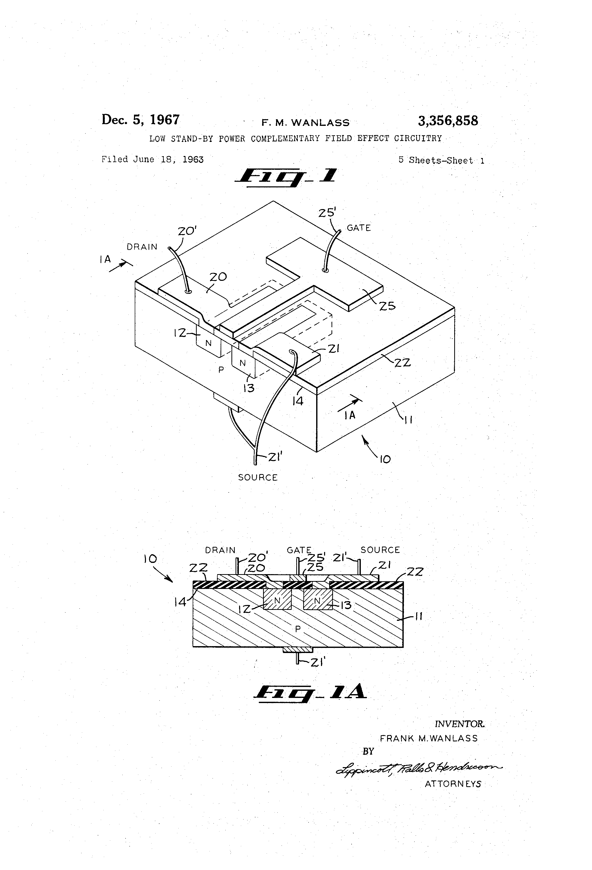
(1)
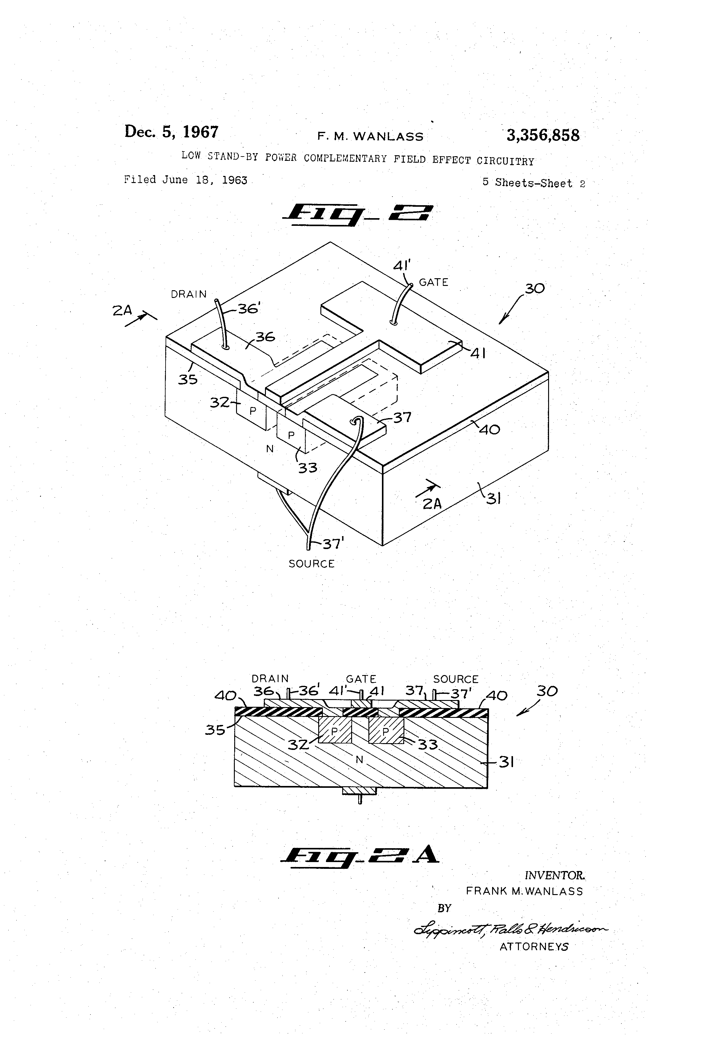
(2)
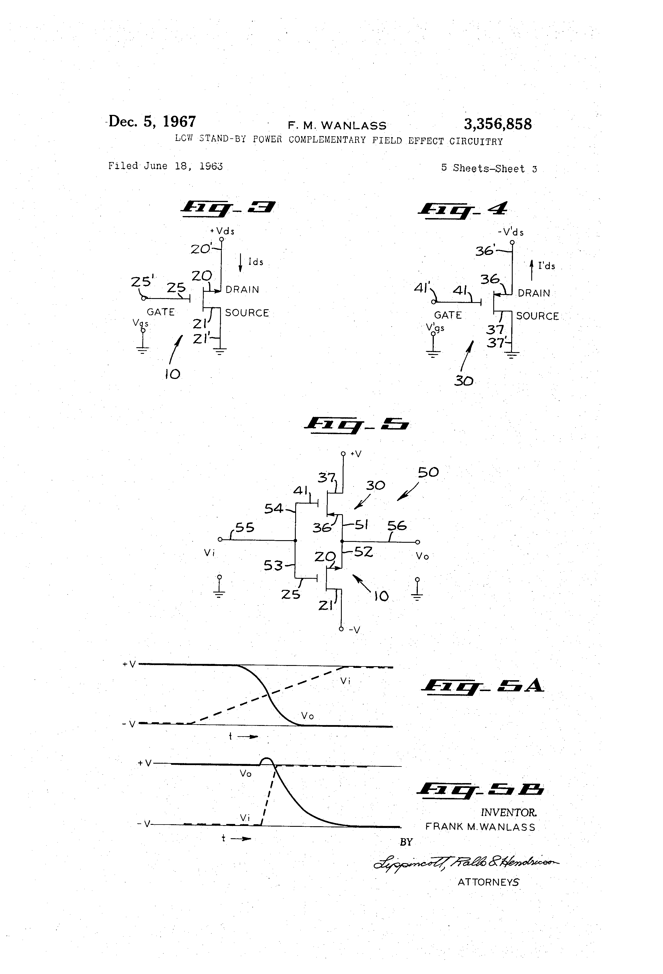
(3)

(4)

(5)
(6)

(7)
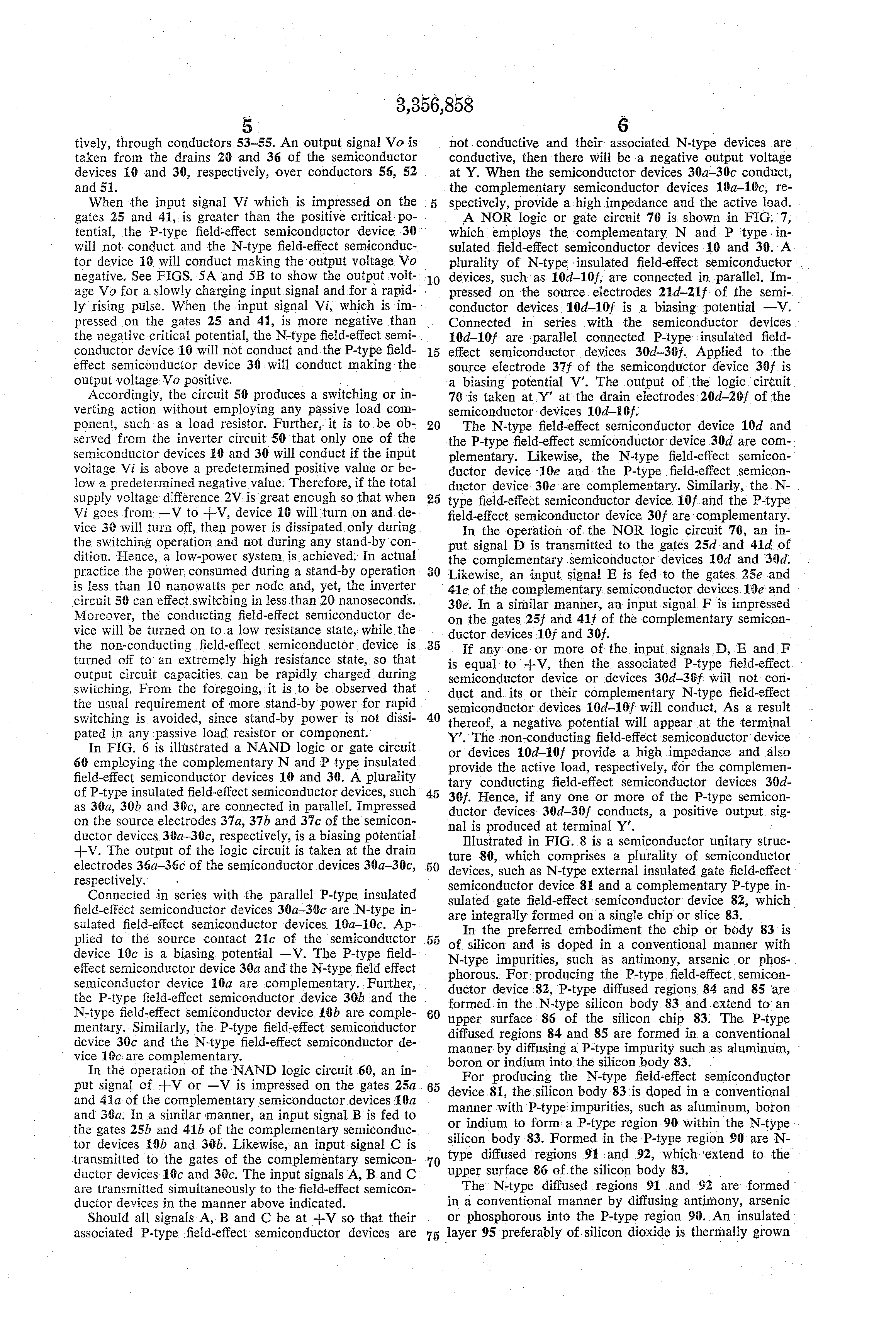
(8)

(9)

(10)
参考资料:
[1] 宋继强. 智能时代的芯片技术演进[J]. 科技导报, 2019, 37(3): 66-68.
doi: 10.3981/j.issn.1000-7857.2019.03.010
http://www.kjdb.org/CN/abstract/abstract15236.shtml
Intel得出的结论是,CMOS功耗和性能表现要优于大部分半导体元器件。至少在最近的10年里,还是要以CMOS为主来制造芯片,其他的新技术可以与CMOS混合使用以提高性能、降低功耗或降低价格。
[2] 宋德生. 信息革命的技术源流[M]. 成都: 四川人民出版社, 1986-04.
[3] Frank Wanlass, National Inventors Hall of Fame
https://www.invent.org/inductees/frank-wanlass
[4] 2022-01-20,萨支唐/Sah, Chih-Tang/仲佰,中国大百科全书,第三版网络版[DB/OL]
https://www.zgbk.com/ecph/words?SiteID=1&ID=116722&Type=bkzyb&SubID=61860
[5] Chih‐Tang Sah, 2012, Celebrated Members 著名会员
https://eds.ieee.org/members/celebrated-members
[6] Electronic Engineering Journal, Steven Leibson, 2023-04-10, A Brief History of the MOS transistor, Part 3: Frank Wanlass – MOS Evangelist, Inventor of CMOS
[7] 1963: COMPLEMENTARY MOS CIRCUIT CONFIGURATION IS INVENTED
FRANK WANLASS INVENTS THE LOWEST POWER LOGIC CONFIGURATION BUT PERFORMANCE LIMITATIONS IMPEDE EARLY ACCEPTANCE OF TODAY'S DOMINANT MANUFACTURING TECHNOLOGY.
https://www.computerhistory.org/siliconengine/complementary-mos-circuit-configuration-is-invented/
[8] TIMELINE, Computer History Museum
https://www.computerhistory.org/siliconengine/timeline/
[9] Frank Wanlass, Sah Chih-Tang (萨支唐). Nanowatt logic using field-effect metal-oxide semiconductor triodes [C]. 1963 IEEE International Solid-State Circuits Conference. Digest of Technical Papers: 32-33. 1963-02-20 下午
doi: 10.1109/ISSCC.1963.1157450
https://ieeexplore.ieee.org/document/1157450
https://ieeexplore.ieee.org/stamp/stamp.jsp?tp=&arnumber=1157450
[10] Wanlass, F. M "Low Stand-By Power Complementary Field Effect Circuitry." U. S. Patent 3,356,858 (Filed June 18, 1963. Issued December 5, 1967).
https://image-ppubs.uspto.gov/dirsearch-public/print/downloadPdf/3356858
[11] Wei Cao, Huiming Bu, Maud Vinet, Min Cao, Shinichi Takagi, Sungwoo Hwang, Tahir Ghani, Kaustav Banerjee. The future transistors [J]. Nature, 2023, 620(7974): 501–515. 16 August 2023
doi: 10.1038/s41586-023-06145-x
https://www.nature.com/articles/s41586-023-06145-x
[12] Sah Chih-Tang (萨支唐). Evolution of the MOS transistor-from conception to VLSI [J]. Proceedings of the IEEE, 1988, 76(10): 1280 - 1326. October 1988
doi: 10.1109/5.16328
https://ieeexplore.ieee.org/document/16328
[13] Gordon E. Moore. The role of Fairchild in silicon technology in the early days of "Silicon Valley" [J]. Proceedings of the IEEE, 1998, 86(1): 53-62. January 1998
doi: 10.1109/5.658759
https://ieeexplore.ieee.org/document/658759
https://ieeexplore.ieee.org/stamp/stamp.jsp?tp=&arnumber=658759
相关链接:
[1] 2023-09-05,[小资料] 1963年霍夫施泰因(Steven Hofstein)、海曼(Frederic Heiman)的MOS场效应
https://blog.sciencenet.cn/blog-107667-1401577.html
[2] 2023-09-04,[小资料] 1960年阿塔拉(Martin Atalla)、江大原(Dawon Kahng)申请的MOS场效应管专利(图
https://blog.sciencenet.cn/blog-107667-1401453.html
[3] 2023-09-03,[小资料] 1922~23年洛舍夫(Oleg Vladimirovich Losev)发现固体放大作用
https://blog.sciencenet.cn/blog-107667-1401338.html
[4] 2023-09-02,[小资料] 1935年海尔(Oskar Heil)的场效应管专利(图片)
https://blog.sciencenet.cn/blog-107667-1401242.html
[5] 2023-09-01,[小资料] 1926年利林费尔德(Julius Edgar Lilienfeld)的场效应半导体专利(图片)
https://blog.sciencenet.cn/blog-107667-1401136.html
[6] 2023-08-31,[小资料] 1949年肖克莱(William Bradford Shockley)的结型晶体管论文的引言(图片)和图片页
https://blog.sciencenet.cn/blog-107667-1401002.html
[7] 2023-08-30,[小资料] 1948年巴丁、布拉坦(Bardeen, Brattain)的点接触晶体管专利(图片)
https://blog.sciencenet.cn/blog-107667-1400907.html
[8] 2023-08-29,[小资料] 1959年霍尔尼(Jean Amedee Hoerni)的平面工艺专利(图片)
https://blog.sciencenet.cn/blog-107667-1400737.html
[9] 2023-08-28,[小资料] 1959年诺伊斯(Robert Norton Noyce)的集成电路专利(图片)
https://blog.sciencenet.cn/blog-107667-1400618.html
[10] 2023-08-27,[小资料] 1959年基尔比(Jack St. Clair Kilby)的集成电路专利(图片)
https://blog.sciencenet.cn/blog-107667-1400524.html
[11] 2023-08-21,[征求意见稿] “半电路、半电磁场”电路:目标和现状
https://blog.sciencenet.cn/blog-107667-1399839.html
[12] 2023-08-02,[小资料] 1952年杜默(G. W. A. Dummer)提出“集成电路概念 Integrated Circuit Concept”
https://blog.sciencenet.cn/blog-107667-1397631.html
[13] 2023-05-01,“五一”国际劳动节:真空管 → 晶体管、集成电路 → “半电路、半电磁场”电路 → ……
https://blog.sciencenet.cn/blog-107667-1386442.html
[14] 2019-07-17,[求助] 集成电路 Integrated Circuit 当前最新技术资料?
https://blog.sciencenet.cn/blog-107667-1189948.html
[15] 2019-07-14,有关集成电路 Integrated Circuit 的网页
https://blog.sciencenet.cn/blog-107667-1189467.html
[16] 2019-03-17,[建议] 关于集成电路中研制可变电阻的建议
https://blog.sciencenet.cn/blog-107667-1168144.html
[17] 2019-07-07,有关 Geoffrey W. A. Dummer 先生的网页
https://blog.sciencenet.cn/blog-107667-1188470.html
[18] 2019-07-13,有关 Mervin Joe Kelly 先生的网页
https://blog.sciencenet.cn/blog-107667-1189385.html
[19] 2019-07-01,[请教] 量子集成电路、量子芯片 Quantum Chip 今后30年内的实用前景?
https://blog.sciencenet.cn/blog-107667-1187623.html
[20] 2021-08-10,[求证] ASML 腾飞的技术原因是什么?【immersion system】
https://blog.sciencenet.cn/blog-107667-1299147.html
[21] 2022-09-24, 《信息革命的技术源流》第三轮阅读:创新真难!
https://blog.sciencenet.cn/blog-107667-1356669.html
感谢您的指教!
感谢您指正以上任何错误!
感谢您提供更多的相关资料!
https://m.sciencenet.cn/blog-107667-1401741.html
上一篇:[小资料] 1963年霍夫施泰因(Steven Hofstein)、海曼(Frederic Heiman)的MOS场效应
下一篇:[小资料] 1966年鲍尔(Robert W. Bower)申请的 MOSFET 自对准栅极工艺专利(图片)