博文
新材料将使局部可变通的二极管成为可能
 精选
精选
||
新材料将使局部可变通的二极管成为可能
诸平


据德国慕尼黑工业大学(Technical University of Munich简称TUM)2022年11月3日报道,新材料将使局部可变通的二极管成为可能(New material will make locally flexible diodes possible)。
研究人员发现了具有巨大电子应用潜力的新材料(Researchers find new material with significant potential for electronics applications)
二极管允许电流定向流动。没有它们,现代电子产品将是不可想象的。到目前为止,它们必须由两种具有不同特性的材料制成。慕尼黑工业大学(TUM)领导的一个研究小组现在发现了一种材料,这种材料可以制造出温度简单变化的二极管。相关研究结果于2022年10月25日已经在《先进材料》(Advanced Materials)杂志网站发表——Anna Vogel, Alfred Rabenbauer, Philipp Deng, Ruben Steib, Thorben Böger, Wolfgang G. Zeier, Renée Siegel, Jürgen Senker, Dominik Daisenberger, Katharina Nisi, Alexander W. Holleitner, Janio Venturini, Tom Nilges. A Switchable One-Compound Diode. Advanced Materials, First published: 25 October 2022. DOI: 10.1002/adma.202208698. https://onlinelibrary.wiley.com/doi/10.1002/adma.202208698
参与此项研究的除了来自TUM的研究人员之外,还有来自德国明斯特大学(University of Münster, Germany)、德国拜罗伊特大学(University of Bayreuth, Germany)以及英国钻石光源(Diamond Light Source, Harwell Science and Innovation Campus, Didcot, Oxfordshire, UK)的研究人员。
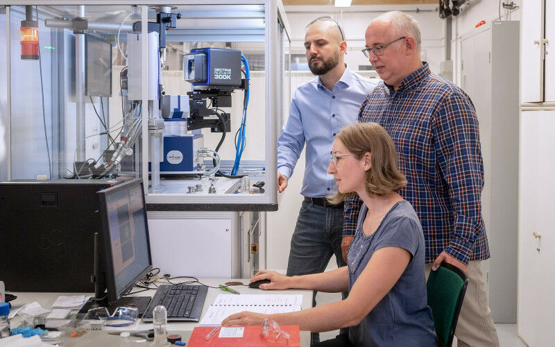
上述图1(Fig. 1)显示贾尼奥·文图里尼(Janio Venturini)博士(左)、汤姆·尼尔格斯(Tom Nilges)教授和第一作者安娜·沃格尔(Anna Vogel)在用于确定晶体结构的测量设备前。
制造二极管通常涉及组合两种具有不同特性的半导体材料。在大多数情况下,这些是硅的改性形式,其中添加了不同的元素以产生所需的特性。这个过程被称为掺杂(doping)。
将自由电子添加到材料中的磷(P)、砷(As或锑(Sb)的掺杂被称为n型掺杂(n-type doping)。n指带负电的电子(negatively charged electrons)。相比之下,硼(B)、铝(Al)和镓(Ga)结合来自硅的电子,从而产生带正电的空穴(positively charged holes)。该材料是p掺杂的。将这两种材料结合在一起会产生一个二极管,该二极管允许电流仅沿一个方向流动。
图片2(Fig. 2)是安娜·沃格尔在单晶衍射仪上安装单晶。在她的面前,可以看到一个玻璃毛细管,上面有一个直径约0.2 mm的晶体。使用合适的测量辐射记录数据,以便从中确定结构。
温度改变材料特性(Temperature changes material characteristics)
TUM 创新材料合成与表征(Synthesis and Characterisation of Innovative Materials at TUM)教授汤姆·尼尔格斯说:“我们现在发现了一种材料,只需改变温度即可使其成为n型或p型导电材料。” 研究人员已经能够证明,仅仅几度的温度变化就足以产生这种效果——并且可以在材料内产生温度梯度的功能二极管。
“当材料处于室温时,我们有一个完全正常的p型导体。如果我们随后应用温度梯度,我们可以同时在加热区域产生一个n型导体,”汤姆·尼尔格斯教授解释说。应用的一个重要方面:在室温范围内的效应函数。“如果想要生成二极管,只需几度的局部温升就足够了——在我们的例子中是 22~35 ℃即可。”
对于汤姆·尼尔格斯来说,消除掺杂的需要并不是唯一的优势:“生产的每个二极管始终存在。我们的材料并非如此:随着温度梯度,二极管也会消失。如果再次需要,产生温度梯度就足够了。如果我们考虑二极管的应用范围,例如在太阳能电池或各种电子元件中,这项发明的潜力是显而易见的。”
复杂的成分(Complex composition)
寻找完美材料的工作历时12年之久,该团队现在终于发现了造币金属硫族化物卤化物(coinage metal chalcogenide halide) Ag18Cu3Te11Cl3。它由银(Ag)、铜(Cu)、碲(Te)和氯(Cl)元素组成。研究人员在探索利用热量发电的热电材料时遇到了这类化合物。他们研究的一种材料显示了p-n开关效应(p-n switching effect)。然而,这仅在100 ℃左右的温度范围内观察到,不适合实际应用。
上述图3(Fig. 3)为Ag18Cu3Te11Cl3大晶体,位于石英玻璃安瓿中。在这个安瓿中,所有元素银、铜、碲和卤化物的化合物都是在真空下产生的。
经过广泛的分析和实验,研究人员在Ag18Cu3Te11Cl3中发现了一种显示出预期效果的材料,也适用于常温下的应用。“其他研究小组也在各种材料中发现了这种转换效应,但到目前为止,还没有人能够将其转化为特定的应用,”汤姆·尼尔格斯解释道。
作为下一步,研究人员计划证明他们的材料可用于通过温度变化来制造晶体管。
期待硅太阳能电池的效率显著提高(Anticipating silicon solar cells with significantly improved efficiency)
图4(Fig. 4)为化合物Ag18Cu3Te11Cl3安装在用于测量电子特性的组件上。
本研究得到了慕尼黑工业大学人才工厂计划(TUM Talent factory program)、德国研究基金会(Deutsche Forschungsgemeinschaft简称DFG / German Research Foundation)根据德国卓越战略(Germany’s Excellence Strategy EXC 2089/1-390776260)的资助。
上述介绍,仅供参考。欲了解更多信息,敬请注意浏览原文或者相关报道。
A diode or transistor requires the combination of p- and n-type semiconductors or at least the defined formation of such areas within a given compound. This is a prerequisite for any IT application, energy conversion technology, and electronic semiconductor devices. Since 2009, when the first pnp-switchable compound Ag10Te4Br3 was described, it is in principle possible to fabricate a diode from a single material without adjusting the semiconduction type by a defined doping level. After this discovery, a handful of other materials that are capable of reversibly switching between these two semiconducting stages was reported. In all cases, a structural phase transition accompanied by a dynamic change of charge carriers or a charge density wave (CDW) within certain substructures are responsible for this effect. Unfortunately, a certain feature hinders the application of this phenomenon in convenient devices, namely the pnp-switching temperature, which generally occurs well above room temperature, between 364 and 580 K. This effect is far removed from a suitable operation temperature at ambient conditions. Here, we report on Ag18Cu3Te11Cl3, a room temperature pnp-switching material, and the realization of the first single-material position-independent diode. The title compound shows the highest ever reported Seebeck coefficient drop that takes place within a few Kelvin at room temperature. Combined with its reasonably low thermal conductivity, this material offers great application potential within an easily accessible and applicable temperature window. Ag18Cu3Te11Cl3 and pnp-switching materials have the potential for applications and processes where diodes, transistors, or any defined charge separation with junction formation are utilized.
https://m.sciencenet.cn/blog-212210-1362369.html
上一篇:DNA“纳米转运蛋白”治疗癌症
下一篇:科学需要更好的欺诈检测和更多的举报人