博文
[小资料] 1966年鲍尔(Robert W. Bower)申请的 MOSFET 自对准栅极工艺专利(图片)
||
[小资料] 1966年鲍尔(Robert W. Bower)申请的 MOSFET 自对准栅极工艺专利(图片)
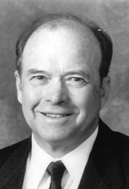
鲍尔 Robert W. Bower, 1936-06-12 ~
https://www.invent.org/inductees/robert-w-bower
一、人类生产的 1022 个晶体管,其中 99.9% 是 MOS器件
在美国工程技术界评出二十世纪最伟大的 20项工程技术成就“Electronics 电子技术”时间表里,《1966 Self-aligned gate process for fabricating field effect transistors 1966年 用于制造场效应晶体管的自对准栅极工艺》内容如下:
1966 Self-aligned gate process for fabricating field effect transistors
In 1966 Dr. Robert W. Bower invents the self-aligned gate process for fabricating field effect transistors, providing the foundation for later developments establishing the core technology for the fabrication of high performance MOS integrated circuits.
1966年 用于制造场效应晶体管的自对准栅极工艺
1966年,Robert W.Bower 博士发明了用于制造场效应晶体管的自对准栅极工艺,为后来的发展奠定了基础,为制造高性能 MOS 集成电路的核心技术奠定了基础。
http://www.greatachievements.org/?id=3956
In 1966, Bower and Dill presented the first publication the self-aligned gate transistor at the International Electron Device Meeting in Washington D.C.. That IEDM publication described the self-aligned gate transistor fabricated with both metal and polysilicon as the gate material and using both ion implantation and diffusion to form the source and drains. This was presentation 16.6 of this IEDM meeting.
1966年,Bower 和 Dill 在华盛顿特区举行的国际电子器件会议上发表了第一份出版物《自对准栅极晶体管》。该 IEDM 出版物描述了以金属和多晶硅为栅极材料,并使用离子注入和扩散形成源极和漏极的自对准栅晶体管。这是本次 IEDM 会议的 16.6 介绍。
http://www.edubilla.com/inventor/robert-w-bower/
Five decades later the industry had shipped 13 sextillion transistors, 99.9 percent of them MOS devices. And the total increases by multiple billions every day.
【截止到2018年】50年后,该行业已经向市场供应了 1.3×10²² 个晶体管,其中 99.9% 是 MOS器件。总的来说,每天都在以几十亿个的速度增长。
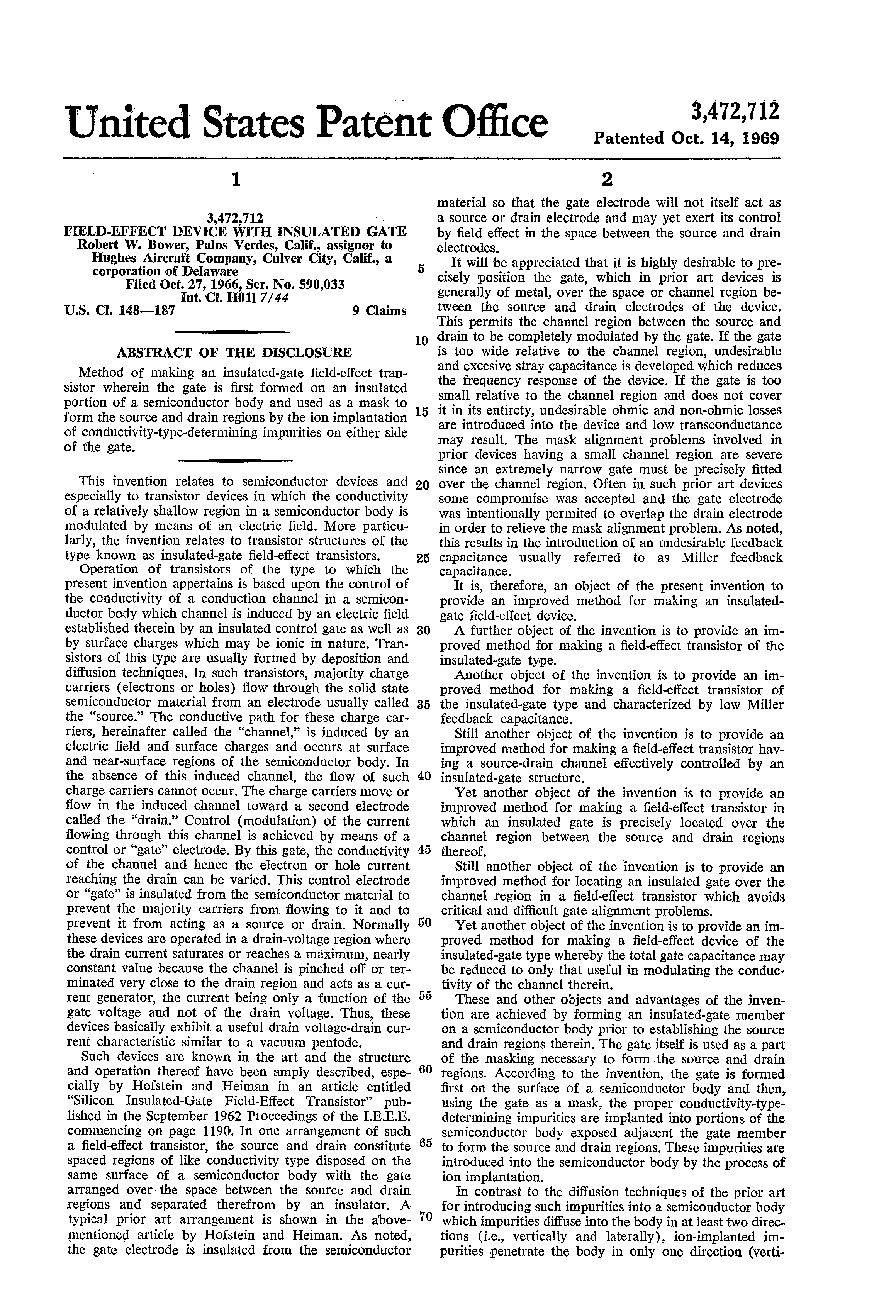
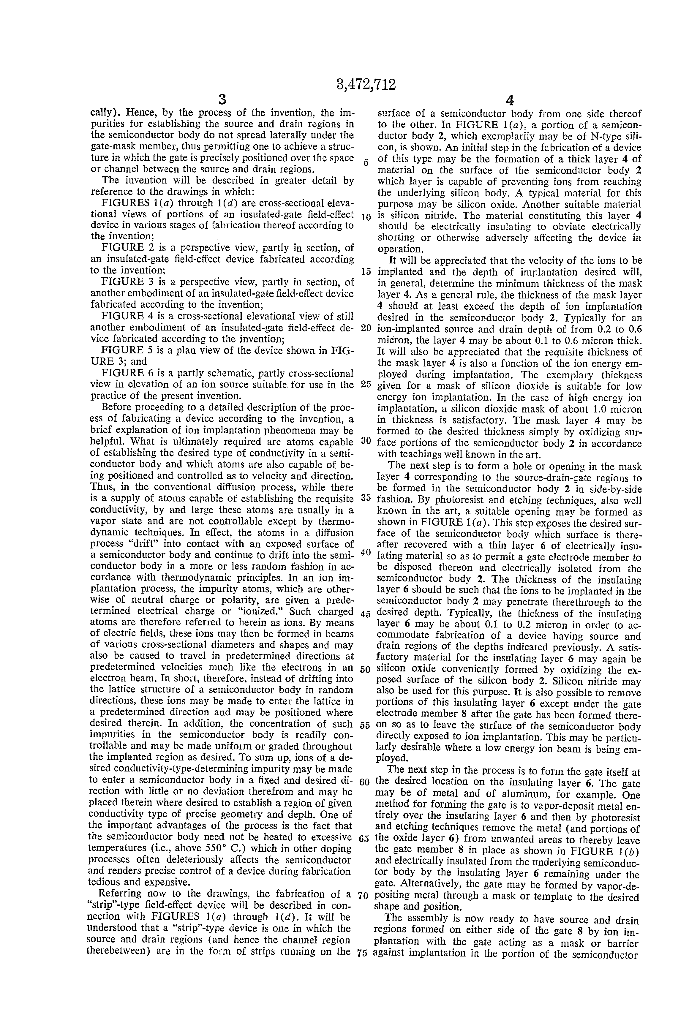
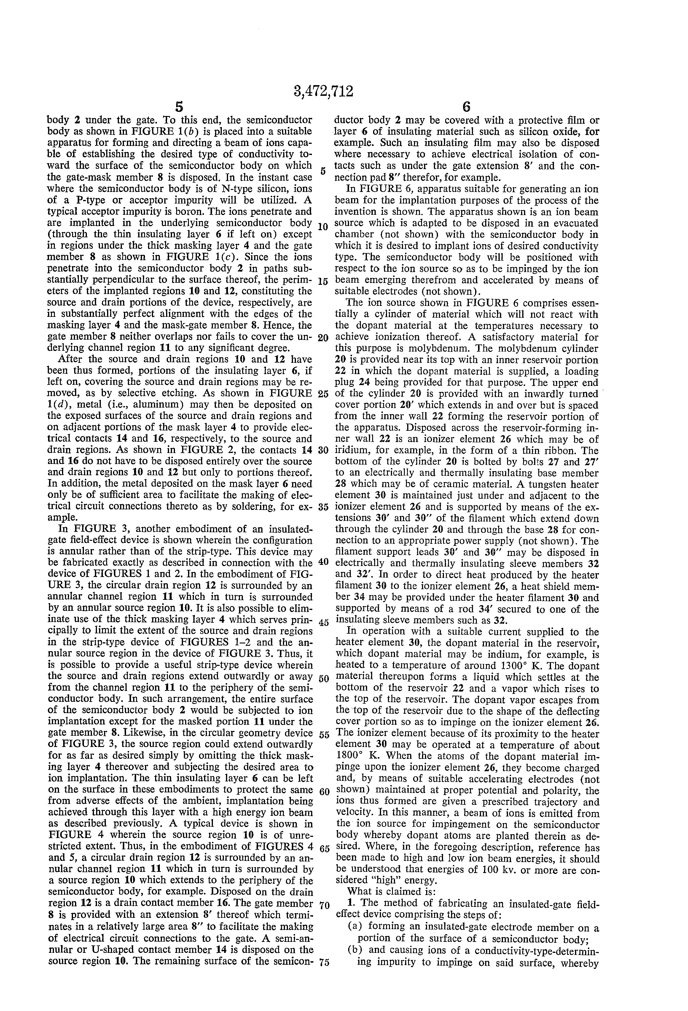
二、1966年鲍尔(Robert W. Bower)申请的MOSFET自对准栅极工艺专利《Field-effect device with insulated gate 绝缘栅场效应器件》
https://image-ppubs.uspto.gov/dirsearch-public/print/downloadPdf/3472712
鲍尔 1966-10-27 申请,1969-10-14 授权的MOSFET自对准栅极工艺专利的美国专利“Field-effect device with insulated gate 绝缘栅场效应器件”(U.S. Patent 3,472,712; Filed Oct. 27, 1966)。
图片形式如下:
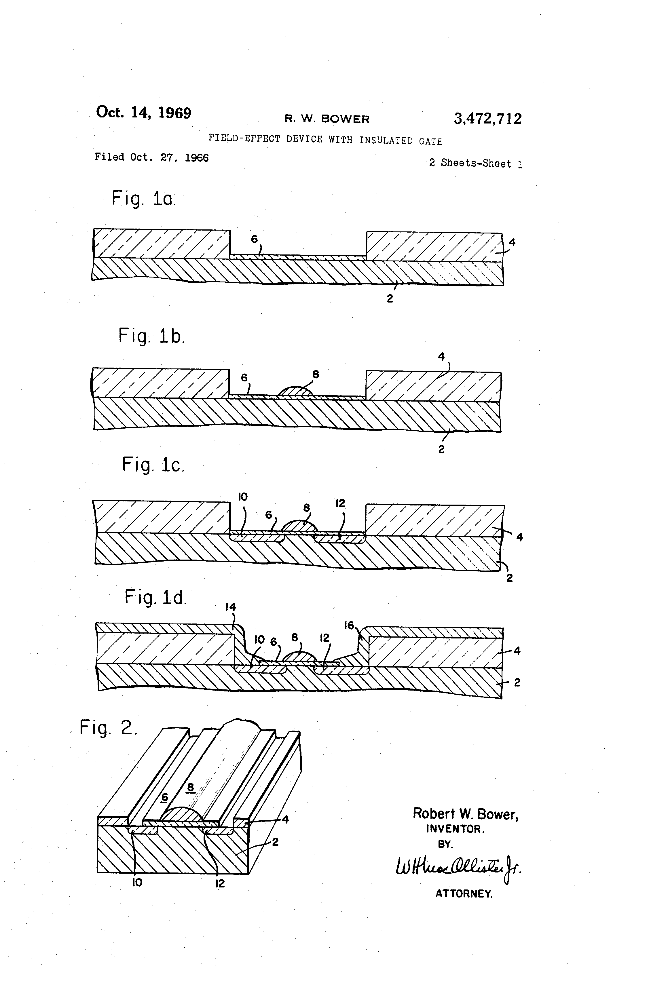
(1)
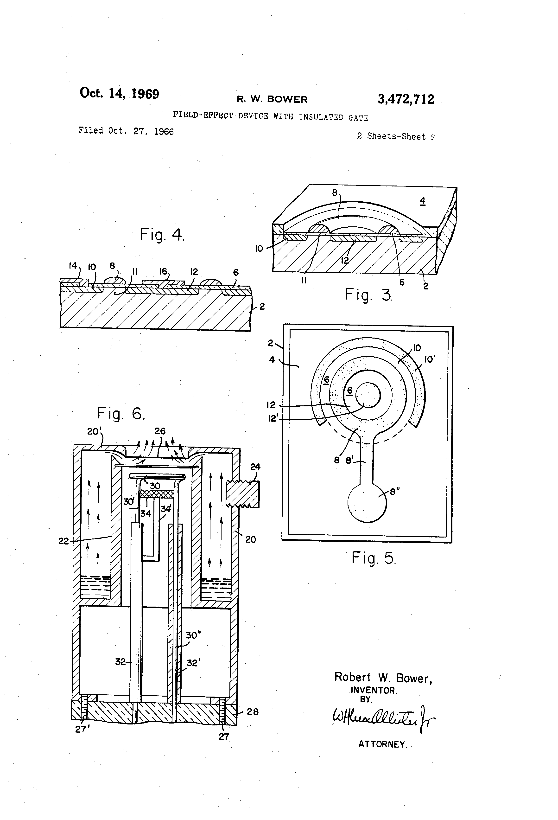
(2)
(3)
(4)
(5)
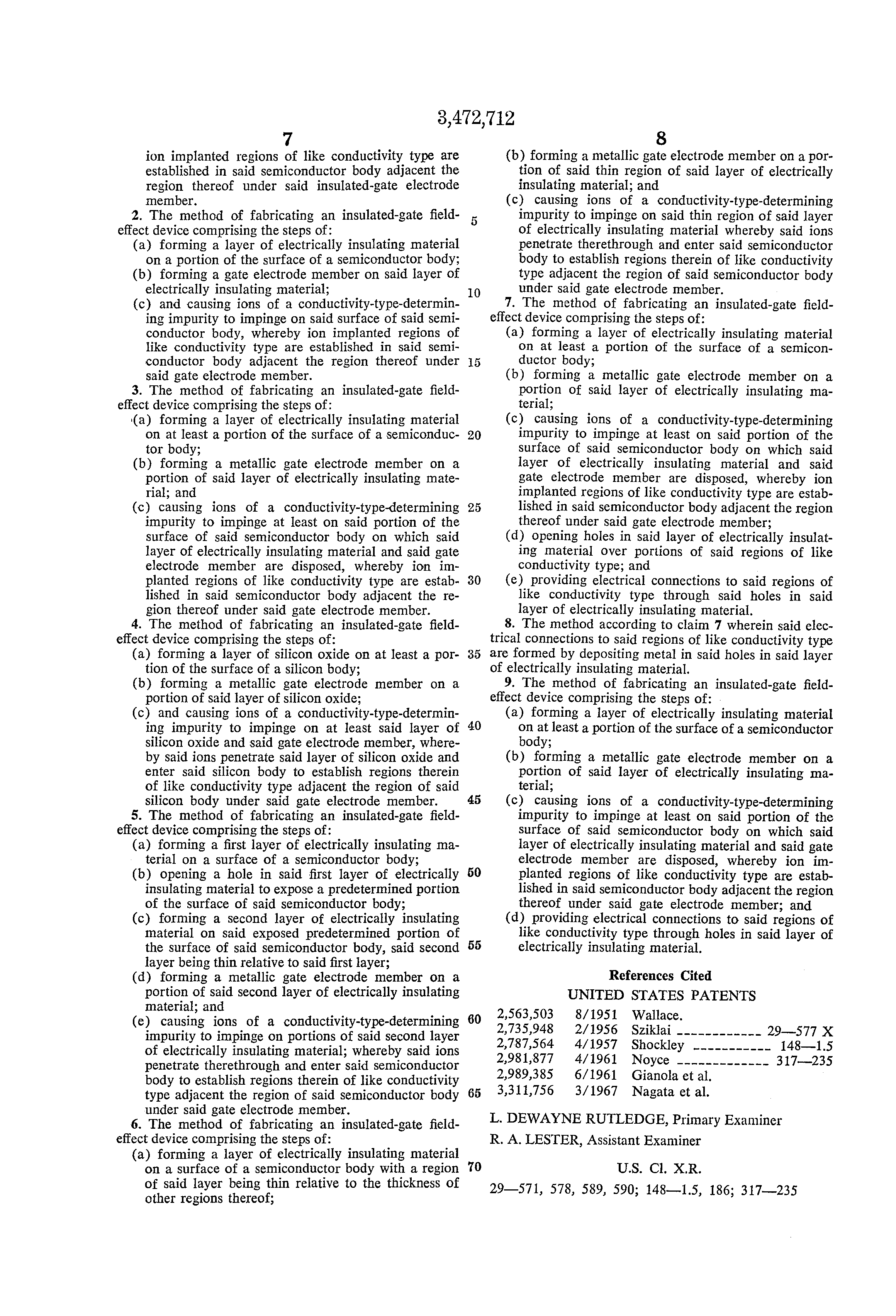
(6)
参考资料:
[1] 宋继强. 智能时代的芯片技术演进[J]. 科技导报, 2019, 37(3): 66-68.
doi: 10.3981/j.issn.1000-7857.2019.03.010
http://www.kjdb.org/CN/abstract/abstract15236.shtml
Intel得出的结论是,CMOS功耗和性能表现要优于大部分半导体元器件。至少在最近的10年里,还是要以CMOS为主来制造芯片,其他的新技术可以与CMOS混合使用以提高性能、降低功耗或降低价格。
[2] 宋德生. 信息革命的技术源流[M]. 成都: 四川人民出版社, 1986-04.
[3] 美国国家工程院. Greatest Engineering Achievements of the Twentieth Century [EB/OL].
http://www.greatachievements.org/
[4] Electronics Timeline, the 20th century's greatest engineering achievements
http://www.greatachievements.org/?id=3956
[5] Robert W. Bower, National Inventors Hall of Fame 国家发明家名人堂
https://www.invent.org/inductees/robert-w-bower
[6] Robert W. Bower - Famous Inventor
http://www.edubilla.com/inventor/robert-w-bower/
[7] 13 sextillion & counting: the long & winding road to the most frequently manufactured human artifact in history, David Laws, 2018-04-02, Computer History Museum
[8] Wei Cao, Huiming Bu, Maud Vinet, Min Cao, Shinichi Takagi, Sungwoo Hwang, Tahir Ghani, Kaustav Banerjee. The future transistors [J]. Nature, 2023, 620(7974): 501–515. 16 August 2023
doi: 10.1038/s41586-023-06145-x
https://www.nature.com/articles/s41586-023-06145-x
[9] Sah Chih-Tang (萨支唐). Evolution of the MOS transistor-from conception to VLSI [J]. Proceedings of the IEEE, 1988, 76(10): 1280 - 1326. October 1988
doi: 10.1109/5.16328
https://ieeexplore.ieee.org/document/16328
[10] Gordon E. Moore. The role of Fairchild in silicon technology in the early days of "Silicon Valley" [J]. Proceedings of the IEEE, 1998, 86(1): 53-62. January 1998
doi: 10.1109/5.658759
https://ieeexplore.ieee.org/document/658759
https://ieeexplore.ieee.org/stamp/stamp.jsp?tp=&arnumber=658759
[11] Patent Public Search Basic (PPUBS Basic)
https://ppubs.uspto.gov/pubwebapp/static/pages/ppubsbasic.html
[12] TIMELINE, Computer History Museum
https://www.computerhistory.org/siliconengine/timeline/
[13] RESOURCES, Computer History Museum
https://www.computerhistory.org/siliconengine/resources/
相关链接:
[1] 2023-09-06,[小资料] 1963年万拉斯(Frank Wanlass)、萨支唐(Chih-Tang Sah)申请的CMOS专利和论文
https://blog.sciencenet.cn/blog-107667-1401741.html
[2] 2023-09-05,[小资料] 1963年霍夫施泰因(Steven Hofstein)、海曼(Frederic Heiman)的MOS场效应
https://blog.sciencenet.cn/blog-107667-1401577.html
[3] 2023-09-04,[小资料] 1960年阿塔拉(Martin Atalla)、江大原(Dawon Kahng)申请的MOS场效应管专利(图
https://blog.sciencenet.cn/blog-107667-1401453.html
[4] 2023-09-03,[小资料] 1922~23年洛舍夫(Oleg Vladimirovich Losev)发现固体放大作用
https://blog.sciencenet.cn/blog-107667-1401338.html
[5] 2023-09-02,[小资料] 1935年海尔(Oskar Heil)的场效应管专利(图片)
https://blog.sciencenet.cn/blog-107667-1401242.html
[6] 2023-09-01,[小资料] 1926年利林费尔德(Julius Edgar Lilienfeld)的场效应半导体专利(图片)
https://blog.sciencenet.cn/blog-107667-1401136.html
[7] 2023-08-31,[小资料] 1949年肖克莱(William Bradford Shockley)的结型晶体管论文的引言(图片)和图片页
https://blog.sciencenet.cn/blog-107667-1401002.html
[8] 2023-08-30,[小资料] 1948年巴丁、布拉坦(Bardeen, Brattain)的点接触晶体管专利(图片)
https://blog.sciencenet.cn/blog-107667-1400907.html
[9] 2023-08-29,[小资料] 1959年霍尔尼(Jean Amedee Hoerni)的平面工艺专利(图片)
https://blog.sciencenet.cn/blog-107667-1400737.html
[10] 2023-08-28,[小资料] 1959年诺伊斯(Robert Norton Noyce)的集成电路专利(图片)
https://blog.sciencenet.cn/blog-107667-1400618.html
[11] 2023-08-27,[小资料] 1959年基尔比(Jack St. Clair Kilby)的集成电路专利(图片)
https://blog.sciencenet.cn/blog-107667-1400524.html
[12] 2023-08-21,[征求意见稿] “半电路、半电磁场”电路:目标和现状
https://blog.sciencenet.cn/blog-107667-1399839.html
[13] 2023-08-02,[小资料] 1952年杜默(G. W. A. Dummer)提出“集成电路概念 Integrated Circuit Concept”
https://blog.sciencenet.cn/blog-107667-1397631.html
[14] 2023-05-01,“五一”国际劳动节:真空管 → 晶体管、集成电路 → “半电路、半电磁场”电路 → ……
https://blog.sciencenet.cn/blog-107667-1386442.html
[15] 2019-07-17,[求助] 集成电路 Integrated Circuit 当前最新技术资料?
https://blog.sciencenet.cn/blog-107667-1189948.html
[16] 2019-07-14,有关集成电路 Integrated Circuit 的网页
https://blog.sciencenet.cn/blog-107667-1189467.html
[17] 2019-03-17,[建议] 关于集成电路中研制可变电阻的建议
https://blog.sciencenet.cn/blog-107667-1168144.html
[18] 2019-07-07,有关 Geoffrey W. A. Dummer 先生的网页
https://blog.sciencenet.cn/blog-107667-1188470.html
[19] 2019-07-13,有关 Mervin Joe Kelly 先生的网页
https://blog.sciencenet.cn/blog-107667-1189385.html
[20] 2019-07-01,[请教] 量子集成电路、量子芯片 Quantum Chip 今后30年内的实用前景?
https://blog.sciencenet.cn/blog-107667-1187623.html
[21] 2021-08-10,[求证] ASML 腾飞的技术原因是什么?【immersion system】
https://blog.sciencenet.cn/blog-107667-1299147.html
[22] 2022-09-24, 《信息革命的技术源流》第三轮阅读:创新真难!
https://blog.sciencenet.cn/blog-107667-1356669.html
感谢您的指教!
感谢您指正以上任何错误!
感谢您提供更多的相关资料!
https://m.sciencenet.cn/blog-107667-1401852.html
上一篇:[小资料] 1963年万拉斯(Frank Wanlass)、萨支唐(Chih-Tang Sah)申请的CMOS专利和论文
下一篇:[小资料] 1966年 ~ 1998年“电子学 Electronics”重要事件