博文
半导体里程_博物馆_1956年 硅片在硅谷首次出现
|||
1956-硅片在硅谷首次出现
肖克利半导体实验室建造了加州北部的第一个原型开发半导体设备来为硅谷训练年轻的工程师和科学家。
1955年9月,威廉萧克利和阿诺贝克曼同意建立肖克利半导体实验室作为贝克曼的部门来“积极、大力开展关于半导体材料的活动”。肖克利在加利福尼亚州山景城圣安东尼奥南部道路租用了391号楼,同时,开始招聘“世界上最有创造力的团队开发、设计、生产晶体管”。他吸引了很多能干的工程师和科学家,其中了解和开发硅相关技术和工艺、扩散技术的戈登·摩尔和罗伯特·伊斯都被他招聘来工作。1956年12月萧克利因为发明晶体管获得了诺贝尔物理学奖,但是,他的助理开始厌倦了他懒散的管理模式。他们也觉得公司应该追求更直接生产硅晶体管的机会而不是期盼遥远的目标“他在实验室将硅应用到电话通讯领域”。
在要求肖克利再雇用一名新的管理后,摩尔、尤利乌斯·伊斯、格里尼克、琼·霍尔尼、克莱纳、拉斯特、罗伯茨8名萧克利员工在1957年9月辞职并创立了美国飞兆半导体公司在帕洛阿尔托。许多来自播实之星的员工随之而来。在未来十年里,快捷半导体成长为在半导体产业最重要的和创新的公司,引导了硅谷其他企业科技和文化,其中超微半导体和英特尔连接技术,但是,他的公司从来没有获得实际的利润。贝克曼在1960年把专利卖给了Clevite公司。萧克利在斯坦福大学成了一个教授的电气工程与应用科学的老师。
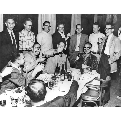
Toasting Shockley's Nobel Prize award at Rickey's Hotel, Palo Alto, CA. Celebrants include G. Moore, S. Roberts, R. Noyce, and J. Last
肖克利诺贝尔奖奖在里奇的酒店,帕洛阿尔托约礼,包括穆尔,罗伯茨,诺伊斯,和J·
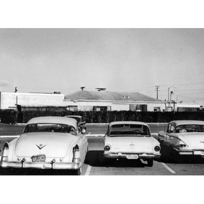
The Shockley Semiconductor Laboratory facility, Mountain View, CA. circa 1960.
肖克利半导体实验室设施,山景,约公元1960。
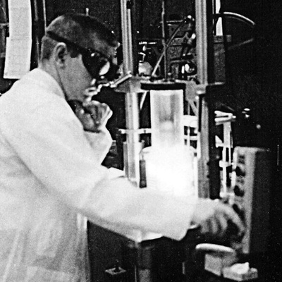
Small-scale silicon zone refining in the Shockley laboratory in Mountain View
小型硅精炼的肖克利实验室在山景
Small-scale silicon zone refining in the Shockley laboratory in Mountain View
小型硅精炼的肖克利实验室在山景
1956 - Silicon Comes to Silicon Valley Shockley Semiconductor Laboratory develops Northern California's first prototype silicon devices while training young engineers and scientists for the future Silicon Valley.
In September 1955 William Shockley and Arnold Beckman agreed to found the Shockley Semiconductor Laboratory as a Division of Beckman Instruments "to engage promptly and vigorously in activities related to semiconductors." Shockley rented a building at 391 South San Antonio Road in Mountain View, California, and began recruiting "the most creative team in the world for developing and producing transistors." He attracted extremely capable engineers and scientists, including Gordon Moore and Robert Noyce, who learned about and developed technologies and processes related to silicon and diffusion while working there. In December 1956 Shockley shared the Nobel Prize in Physics for inventing the transistor, but his staff was becoming disenchanted with his difficult management style. They also felt the company should pursue more immediate opportunities for producing silicon transistors rather than the distant promise of a challenging four-layer p-n-p-n diode he had conceived at Bell Labs for telephone switching applications.
After unsuccessfully asking Beckman to hire a new manager, eight Shockley employees - including Moore and Noyce plus Julius Blank, Victor Grinich, Jean Hoerni, Eugene Kleiner, Jay Last and Sheldon Roberts - resigned in September 1957 and founded the Fairchild Semiconductor Corporation in Palo Alto. Many other employees, from technicians to PhDs, soon followed. Over the next decade, Fairchild grew into of the most important and innovative companies in the semiconductor industry, laying the technological and cultural foundations of Silicon Valley while spinning off dozens of new high-tech start-ups, including Advanced Micro Devices (AMD) and Intel. Shockley continued pursuing his four-layer diode but his company never realized a profit. Beckman sold the operation to Clevite Corporation in 1960. Shockley became a professor of electrical engineering and applied science at Stanford University.
译者:哈尔滨工业大学(威海)电子封装 090840120-王开伟
校对:哈尔滨工业大学(威海)电子封装 090840117-康志龙
https://m.sciencenet.cn/blog-652849-544784.html
上一篇:半导体里程_博物馆_1954_硅晶体管提供优越的工作特性
下一篇:半导体里程_博物馆_1958-硅台面晶体管进入商业生产