博文
半导体里程_博物馆_1966-集成电路计算机辅助设计工具的开发
|||
IBM的工程师们开发了用以减少研发错误和设计时间的计算机辅助电子设计自动化工具。
当集成电路开始包含几百个门电路和数以千计的晶体管时,他们所支持的计算机已经可以完成加快设计速度和减少设计错误的任务了。这个方法被称作CAD(计算机辅助设计)或者EDA(电子设计自动化)。IBM在20世纪50年代末率先开发了在700系列电脑文档下运行的EDA程序。到了1966年,James Koford和他的同事们在IBM纽约州东费西基尔公司用图形显示器采集STL混合电路模块(1964里程碑事件)的图案,检查他们的错误并自动将信息转换为掩膜模式。在Koford加入Fairchild R&D后他又与Hugh Mays 、Ed Jones及其他同事一起将这项程序应用于单片集成电路。他们的努力创造了逻辑模拟软件(FAIRSIM)、测试程序生成器软件以及门列阵和标准单元布局布线软件(1967年里程碑事件),这些为一代又一代的EDA工具打下了坚实的基础。
EDA有两个重要项目源于非主流产业。20世纪60年代,Larry Nagel和Donald Pederson以及后来的贡献者Richard Newton在美国加州大学伯克利分校开发了SPICE(模拟集成电路重点项目)电路仿真程序。1979年,加州理工学院的Lynn Conway of Xerox和Carver Mead在他们论著的《超大规模集成电路系统导论》中描述的一个新方法揭开了系统设计和芯片设计过程秘密。
20世纪80年代,益华电脑和美国新思科技公司受到在柏克莱加州大学(SIS)、洛杉矶加利福尼亚大学(RSAP)和科罗拉多大学(BOLD)所做调查的激发,开始对综合逻辑系统进行商业化的包装。这些和先进的布局布线技术、逻辑模拟技术以及其他厂商已有的设计核查规则共同使集成电路的设计生产能力能够紧跟设备复杂度不断增加的步伐。

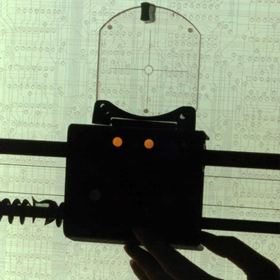
IBM 360/67 仙童公司1967年的以大型计算机为运算动力的CAD设计系统 图1
编辑者:费尔柴尔德摄像机仪器公司
掩模草图数字化手绘系统工具 图2
提供者:因特尔公司
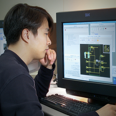
20世纪80年代基于集成电路CAD设计系统的工作站 图3

米德和加威的成就获得了1981年的美国电子奖 图4
译者:哈尔滨工业大学(威海)电子封装 090840213-邱东阳
校对:哈尔滨工业大学(威海)电子封装 090840229-朱泯西
版权 copyright by www.computerhistory.org
1966 - Computer Aided Design Tools Developed for ICs
IBM engineers pioneer computer-aided electronic design automation tools for reducing errors and speeding design time.
IBM 360/67 mainframe-powered CAD system at Fairchild in 1967
Credit: Fairchild Camera & Instrument Corporation
Mask layout drawing hand digitizing system tool
Courtesy of: Intel Corporation
Workstation-based integrated circuit CAD system 1980s
1981 Electronics Award for Achievement to Conway and Mead
As ICs began to incorporate hundreds of gates and thousands of transistors, the computers they enabled were harnessed to speed the design task and eliminate errors. This process is called CAD (Computer Aided Design) or EDA (Electronic Design Automation). IBM pioneered EDA in the late 1950s with documentation of the 700 series computers. By 1966 James Koford and his colleagues at IBM Fishkill were capturing SLT hybrid circuit module (1964 Milestone) designs on graphical displays, checking them for errors and automatically converting the information into mask patterns. After Koford joined Fairchild R&D he worked with Hugh Mays, Ed Jones, and others to apply this process to monolithic ICs. Their efforts created logic simulators (FAIRSIM), test program generators, and place and route software for gate arrays and standard cells (1967 Milestone) that laid the ground work for generations of EDA tools.
Two important EDA projects originated outside the mainstream of the industry. Larry Nagel and Donald Pederson, with later contributions by Richard Newton, at U.C. Berkeley developed the SPICE (Simulation Program with IC Emphasis) circuit simulation program in the 1960s. A new methodology described in the 1979 Introduction to VLSI Systems by Lynn Conway of Xerox, PARC and Carver Mead of California Institute of Technology demystified the process of chip design for system designers.
Commercial logic synthesis packages from Cadence and Synopsys in the 1980s were stimulated by research at U.C. Berkeley (SIS), U.C.L.A. (RASP), and University of Colorado, Boulder (BOLD). These, together with advancements in place and route, logic simulation, and design rule verification from other vendors, allowed IC design productivity to keep pace with increasing device complexity.
https://m.sciencenet.cn/blog-652849-545460.html
上一篇:半导体-博物馆-1967-核心设备供应商改变工业动向
下一篇:半导体里程_博物馆_1966-半导体读写存储器